
Manual


SiGe, High-Linearity, 2300MHz to 4000MHz
Downconversion Mixer with LO Buffer
MAX19998
_______________________________________________________________________________________ 7
Note 5: Not production tested.
Note 6: Operation outside this range is possible, but with degraded performance of some parameters. See the Typical
Operating Characteristics.
Note 7: All limits reflect losses of external components, including a 0.8dB loss at f
IF
= 300MHz due to the 4:1 impedance trans-
former. Output measurements were taken at IF outputs of the Typical Application Circuit.
Note 8: Guaranteed by design and characterization.
Note 9: 100% production tested for functional performance.
Note 10: Maximum reliable continuous input power applied to the RF port of this device is +12dBm from a 50I source.
Note 11: Measured with external LO source noise filtered so that the noise floor is -174dBm/Hz. This specification reflects the
effects of all SNR degradations in the mixer including the LO noise, as defined in Application Note 2021: Specifications
and Measurement of Local Oscillator Noise in Integrated Circuit Base Station Mixers.
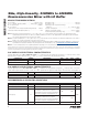
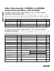
5.0V SUPPLY AC ELECTRICAL CHARACTERISTICS—f
RF
= 2300MHz to 2900MHz,
HIGH-SIDE LO INJECTION (continued)
(Typical Application Circuit, with tuning elements outlined in Table 1, R1 = 698ω, R2 = 604ω, V
CC
= 4.75V to 5.25V, RF and LO ports
are driven from 50I sources, P
LO
= -3dBm to +3dBm, P
RF
= -5dBm, f
RF
= 2300MHz to 2900MHz, f
IF
= 300MHz, f
LO
= 2600MHz
to 3200MHz, f
RF
< f
LO
, T
C
= -40NC to +85NC. Typical values are for T
C
= +25NC, V
CC
= 5.0V, P
RF
= -5dBm, P
LO
= 0dBm, f
RF
=
2600MHz, f
LO
= 2900MHz, f
IF
= 300MHz, unless otherwise noted. (Note 7)
PARAMETER SYMBOL CONDITIONS MIN TYP MAX UNITS
IIP3 Variation with T
C
f
RF
= 2300MHz to 2900MHz, f
RF1
- f
RF2
= 1MHz,
P
RF1
= P
RF2
= -5dBm/tone, T
C
= -40NC to +85NC
Q0.2
dBm
Single-Sideband Noise Figure NF
SSB
No blockers present 10.0 dB
Noise Figure Temperature
Coefficient
TC
NF
Single sideband, no blockers present,
T
C
= -40NC to +85NC
0.018
dB/NC
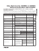
2LO - 2RF Spur Rejection 2 x 2 f
SPUR
= f
LO
- 50MHz
P
RF
= -10dBm 77
dBc
P
RF
= -5dBm 72
3LO - 3RF Spur Rejection 3 x 3 f
SPUR
= f
LO
- 100MHz
P
RF
= -10dBm 86
dBc
P
RF
= -5dBm 76
RF Input Return Loss RL
RF
LO on and IF terminated into a matched
impedance
30 dB
LO Input Return Loss RL
LO
RF and IF terminated into a matched
impedance
18 dB
IF Output Impedance Z
IF
Nominal differential impedance at the IC’s IF
outputs
200
I
IF Output Return Loss RL
IF
RF terminated into 50I,
LO driven by 50I source,
IF transformed to 50I
using external compo-
nents shown in the Typical
Application Circuit. See
the Typical Operating
Characteristics for perfor-
mance vs. inductor values.
f
IF
= 450MHz,
L1 = L2 = 120nH
25
dB
f
IF
= 350MHz,
L1 = L2 = 270nH
25
f
IF
= 300MHz,
L1 = L2 = 390nH
25
RF-to-IF Isolation P
LO
= +3dBm 45 dB
LO Leakage at RF Port P
LO
= +3dBm -28.8 dBm
2LO Leakage at RF Port P
LO
= +3dBm -42.3 dBm
LO Leakage at IF Port P
LO
= +3dBm -26.3 dBm