
Manual


MAX19997A
Dual, SiGe High-Linearity, 1800MHz to 2900MHz
Downconversion Mixer with LO Buffer
2 _______________________________________________________________________________________
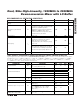
ABSOLUTE MAXIMUM RATINGS
+5.0V SUPPLY DC ELECTRICAL CHARACTERISTICS
(
Typical Application Circuit
optimized for the standard RF band (see Table 1), no input RF or LO signals applied, V
CC
= +4.75V to
+5.25V, T
C
= -40°C to +85°C. Typical values are at V
CC
= +5.0V, T
C
= +25°C, unless otherwise noted. R1, R4 = 750Ω, R2, R5 =
698Ω.)
Stresses beyond those listed under “Absolute Maximum Ratings” may cause permanent damage to the device. These are stress ratings only, and functional
operation of the device at these or any other conditions beyond those indicated in the operational sections of the specifications is not implied. Exposure to
absolute maximum rating conditions for extended periods may affect device reliability.
V
CC
to GND...........................................................-0.3V to +5.5V
RF_, LO to GND.....................................................-0.3V to +0.3V
IFM_, IFD_, IFM_SET, IFD_SET, LO_ADJ_M,
LO_ADJ_ to GND ...................................-0.3V to (V
CC
+ 0.3V)
RF_, LO Input Power ......................................................+15dBm
RF_, LO Current (RF and LO is DC
shorted to GND through balun)................................... ...50mA
Continuous Power Dissipation (Note 1) ..............................8.7W
θ
JA
(Notes 2, 3)..............................................................+38°C/W
θ
JC
(Notes 1, 3)...............................................................7.4°C/W
Operating Case Temperature Range
(Note 4) ...................................................T
C
= -40°C to +85°C
Junction Temperature......................................................+150°C
Storage Temperature Range .............................-65°C to +150°C
Lead Temperature (soldering, 10s) .................................+300°C
PARAMETER SYMBOL CONDITIONS MIN TYP MAX UNITS
Supply Voltage V
CC
3.0 3.3 3.6 V
Supply Current I
CC
Total supply current, V
CC
= +3.3V 279 310 mA
+3.3V SUPPLY DC ELECTRICAL CHARACTERISTICS
(
Typical Application Circuit
optimized for the standard RF band (see Table 1), no input RF or LO signals applied, V
CC
= +3.0V to
+3.6V, T
C
= -40°C to +85°C. Typical values are at V
CC
= +3.3V, T
C
= +25°C, unless otherwise noted. R1, R4 = 1.1kΩ, R2, R5 =
845Ω.)
PARAMETER SYMBOL CONDITIONS MIN TYP MAX UNITS
Supply Voltage V
CC
4.75 5.00 5.25 V
Supply Current I
CC
Total supply current 388 420 mA
Note 1: Based on junction temperature T
J
= T
C
+ (θ
JC
x V
CC
x I
CC
). This formula can be used when the temperature of the exposed
pad is known while the device is soldered down to a PCB. See the
Applications Information
section for details. The junction
temperature must not exceed +150°C.
Note 2: Junction temperature T
J
= T
A
+ (θ
JC
x V
CC
x I
CC
). This formula can be used when the ambient temperature of the PCB is
known. The junction temperature must not exceed +150°C.
Note 3: Package thermal resistances were obtained using the method described in JEDEC specification JESD51-7, using a four-
layer board. For detailed information on package thermal considerations, refer to www.maxim-ic.com/thermal-tutorial
.
Note 4: T
C
is the temperature on the exposed pad of the package. T
A
is the ambient temperature of the device and PCB.