
Instruction Manual

MAX1471
For example, if data is being received at 315MHz, the
crystal frequency is 9.509375MHz. Dividing the crystal
frequency by 100kHz and rounding to the nearest inte-
ger gives 95, or 0x5F hex. So for 315MHz, 0x5F would
be written to the oscillator frequency register.
AGC Dwell Timer Register (Address: 0xA)
The AGC dwell timer holds the AGC in low-gain state
for a set amount of time after the power level drops
below the AGC switching threshold. After that set
amount of time, if the power level is still below the AGC
threshold, the LNA goes into high-gain state. This is
important for ASK since the modulated data may have
a high level above the threshold and a low level below
the threshold, which without the dwell timer would
cause the AGC to switch on every bit.
The AGC dwell time is dependent on the crystal fre-
quency and the bit settings of the AGC dwell timer reg-
ister. To calculate the dwell time, use the following
equation:
where Reg 0xA is the value of register 0xA in decimal.
To calculate the value to write to register 0xA, use the
following equation and use the next integer higher than
the calculated result:
Reg 0xA ≥ 3.3 x log
10
(Dwell Time x f
XTAL
)
For Manchester Code (50% duty cycle), set the dwell
time to at least twice the bit period. For nonreturn-to-
zero (NRZ) data, set the dwell to greater than the peri-
od of the longest string of zeros or ones. For example,
using Manchester code at 315MHz (f
XTAL
=
9.509375MHz) with a data rate of 4kbps (bit period =
125µs), the dwell time needs to be greater than 250µs:
Reg 0xA ≥ 3.3 x log
10
(250µs x 9.509375MHz) ≈11.14
Choose the register value to be the next integer value
higher than 11.14, which is 12 or 0x0C hex.
The default value of the AGC dwell timer on power-up
or reset is 0x0D.
D
f
well Time
Reg0xA
XTAL
=
2
315MHz/434MHz Low-Power, 3V/5V
ASK/FSK Superheterodyne Receiver
18 ______________________________________________________________________________________
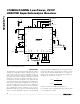
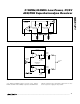
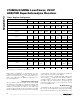
Figure 11. Read Command in 3-Wire Interface
0 0 1 0 0 0 0 0 0 0 0 0A3 A2 A1 A0
READ
COMMAND
ADDRESS DATA
DIO
R7 R6 R5 R4 R3 R2 R1 R0 R0R7
REGISTER DATA
REGISTER
DATA
16 BITS OF DATA
CS
SCLK
0 0 1 0 0 0 0 0 0 0 0 0A3 A2 A1 A0 R7 R6 R5 R4 R3 R2 R1 A3
8 BITS OF DATA
READ
COMMAND
ADDRESS DATA
REGISTER DATA
DIO
CS
SCLK
Table 3. Command Bits
C[3:0] DESCRIPTION
0x0 No operation
0x1 Write data
0x2 Read data
0x3 Master reset
0x4–0xF Not used