
Instruction Manual

Discontinuous Receive Mode (DRX = 1)
In the discontinuous receive mode (DRX = 1), the
power signals of the different modules of the MAX1471
toggle between OFF and ON, according to internal
timers t
OFF
, t
CPU
, and t
RF
. It is also necessary to write
the frequency divisor of the external crystal in the oscil-
lator frequency register (register 0x3). This number is
the integer result of f
XTAL
/ 100kHz. Before entering the
discontinuous receive mode for the first time, it is also
necessary to calibrate the timers (see the Calibration
section).
The MAX1471 uses a series of internal timers (t
OFF
,
t
CPU
, and t
RF
) to control its power-up. The timer
sequence begins when both CS and DIO are one. The
MAX1471 has an internal pullup on the DIO pin, so the
user must tri-state the DIO line when CS goes high.
The external CPU can then go to a sleep mode during
t
OFF
. A high-to-low transition on DIO, or a low level on
DIO serves as the wake-up signal for the CPU, which
must then start its wake-up procedure, and drive DIO
low before t
LOW
expires (t
CPU
+ t
RF
). Once t
RF
expires,
the MAX1471 enables the FSKOUT and/or ASKOUT
data outputs. The CPU must then keep DIO low for as
long as it may need to analyze any received data.
Releasing DIO causes the MAX1471 to pull up DIO,
reinitiating the t
OFF
timer.
Oscillator Frequency Register (Address: 0x3)
The MAX1471 has an internal frequency divider that
divides down the crystal frequency to 100kHz. The
MAX1471 uses the 100kHz clock signal when calibrating
itself and also to set the image-rejection frequency. The
hexadecimal value written to the oscillator frequency reg-
ister is the nearest integer result of f
XTAL
/ 100kHz.
MAX1471
315MHz/434MHz Low-Power, 3V/5V
ASK/FSK Superheterodyne Receiver
______________________________________________________________________________________ 17
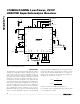
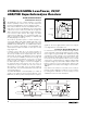
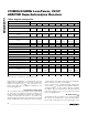
Figure 9. Data Input Diagram
SCLK
A2 A1 D0
ADDRESS
DATA
DIO C3 A3C0C1C2 A0 D7 D6 D5 D4 D3 D2 D1
COMMAND
CS
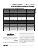
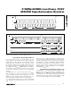
Figure 10. Read Command on a 4-Wire SERIAL Interface
SCLK
CS
0 0 1 0 0 0 0 0 0 0 0 0A3 A2 A1 A0
DIO
C3 C2 C1 C0 A3 A2 A1 A0 D0D7
COMMAND
ADDRESS
DATA
READ
COMMAND
ADDRESS
DATA
ADATA (IF DOUT_ASK = 1)
R7 R6 R5 R4 R3 R2 R1 R0 R0R7
REGISTER DATA
REGISTER
DATA
FDATA (IF DOUT_FSK = 1)
R7 R6 R5 R4 R3 R2 R1 R0 R0R7
REGISTER DATA
REGISTER
DATA