
User guide


MAX1464
Low-Power, Low-Noise Multichannel
Sensor Signal Processor
2 _______________________________________________________________________________________
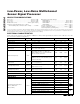
ABSOLUTE MAXIMUM RATINGS
ELECTRICAL CHARACTERISTICS
(V
DDF
= V
DD
= 4.5V to 5.5V, V
SSF
= V
SS
= 0V, f
CLK
= 4.0MHz, T
A
= T
MIN
to T
MAX
. Typical values are at V
DDF
= V
DD
= 5.0V, V
SSF
= V
SS
= 0V,
T
A
= +25°C, unless otherwise noted.) (Note 1)
Stresses beyond those listed under “Absolute Maximum Ratings” may cause permanent damage to the device. These are stress ratings only, and functional
operation of the device at these or any other conditions beyond those indicated in the operational sections of the specifications is not implied. Exposure to
absolute maximum rating conditions for extended periods may affect device reliability.
V
DD
to V
SS
.............................................................-0.3V to +6.0V
V
DDF
to V
SS
...........................................................-0.3V to +6.0V
V
SSF
to V
SS
............................................................-0.3V to +0.3V
All Other Pins to V
SS
...................................-0.3V to (V
DD
+ 0.3V)
Continuous Power Dissipation (T
A
= +70°C)
28-Pin SSOP (derate 9.1mW/°C above +70°C) ..........727mW
Operating Temperature Ranges
MAX1464CAI .....................................................0°C to +70°C
MAX1464C/W.....................................................0°C to +70°C
MAX1464EAI...................................................-40°C to +85°C
MAX1464AAI ................................................-40°C to +125°C
Junction Temperature......................................................+150°C
Storage Temperature Range .............................-65°C to +150°C
Lead Temperature (soldering, 10s) ................................ +300°C
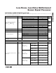
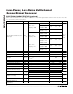
PARAMETER
SYMBOL
CONDITIONS
MIN
TYP
MAX
UNITS
SUPPLY
Supply Voltage V
DD
V
SS
= V
SSF
= 0V 4.5 5.0 5.5 V
FLASH Supply Voltage V
DDF
V
SS
= V
SSF
= 0V 4.5 5.0 5.5 V
Base Operating Current I
BO
CPU stopped (Note 2)
575 720 890
µA
CPU Current I
CPU
All modules off, CPU = on, additive to I
BO
,
I
CPU
= I
DD
+ I
DDF
(Note 3)
540 840 1240
µA
All modules off, ADC = on, ADC clk =
1MHz, additive to I
BO
; the CPU and ADC
are not on at the same time
690 1040 1394
ADC Current (Note 3) I
ADC
All modules off, ADC = on, ADC clk = 7kHz,
additive to I
BO
; the CPU and ADC are not
on at the same time
465 765 1060
µA
DAC Current I
DACn
All modules off, DAC = on, additive to I
BO
(n = 1 or 2) (Note 4)
425 550 730
µA
Large Op-Amp Current I
OPLGn
All modules off, CPU stopped, large op
amp = on (n = 1 or 2)
430 673 1020
µA
Small Op-Amp Current I
OPSMn
All modules off, CPU stopped, small op
amp = on (n = 1 or 2)
110 190 265
µA
POWER-ON RESET
V
DDF
POR Threshold V
DD
> V
DDF
3.6 4.0 4.3 V
V
DDF
POR Hysteresis
-0.85
V
ANALOG INPUT
PGA[4:0] = 00000, CLK[2:0] = 000
430
PGA[4:0] = 01010
,
CLK[2:0] = 000 55
PGA[4:0] = 11111, CLK[2:0] = 000 36
kΩ
PGA[4:0] = 00000, CLK[2:0] = 011 3.4 MΩ
PGA[4:0] = 01010, CLK[2:0] = 011
440
PGA[4:0] = 11111, CLK[2:0] = 011
288
kΩ
PGA[4:0] = 00000, CLK[2:0] = 110 27
PGA[4:0] = 01010, CLK[2:0] = 110 3.5
Differential Input Impedance
(INP1 to INM1 and
INP2 to INM2)
R
DIN
PGA[4:0] = 11111, CLK[2:0] = 110 2.3
MΩ