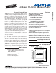
9-2922; Rev 1; 5/04 KIT ATION EVALU E L B AVAILA 65Msps, 12-Bit, IF Sampling ADC ♦ Fully Differential or Single-Ended Analog Input ♦ ♦ ♦ ♦ ♦ ♦ ♦ ♦ Adjustable Full-Scale Analog Input Range Common-Mode Reference Power-Down Mode CMOS-Compatible Outputs in Two’s Complement or Gray Code Data-Valid Indicator Simplifies Digital Interface Out-of-Range Indicator Miniature, 40-Pin Thin QFN Package with Exposed Paddle Evaluation Kit Available (Order MAX1211EVKIT) Ordering Information PART TEMP RANGE PIN-PACKAG
MAX1211 65Msps, 12-Bit, IF Sampling ADC ABSOLUTE MAXIMUM RATINGS VDD to GND ...........................................................-0.3V to +3.6V OVDD to GND........-0.3V to the lower of (VDD + 0.3V) and +3.6V INP, INN to GND ...-0.3V to the lower of (VDD + 0.3V) and +3.6V REFIN, REFOUT, REFP, REFN, COM to GND.....-0.3V to the lower of (VDD + 0.3V) and +3.6V CLKP, CLKN, CLKTYP, G/T, DCE, PD to GND ........-0.3V to the lower of (VDD + 0.3V) and +3.6V D11–D0, I.C., DAV, DOR to GND ............-0.
65Msps, 12-Bit, IF Sampling ADC (VDD = 3.3V, OVDD = 2.0V, GND = 0, REFIN = REFOUT (internal reference), CREFOUT = 0.1µF, CL ≈ 5pF at digital outputs, VIN = 0.5dBFS, CLKTYP = high, DCE = high, PD = low, G/T = low, fCLK = 65MHz (50% duty cycle), CREFP = CREFN = 0.1µF, 1µF in parallel with 10µF between REFP and REFN, CCOM = 0.1µF in parallel with 2.2µF to GND, TA = -40°C to +85°C, unless otherwise noted. Typical values are at TA = +25°C.
MAX1211 65Msps, 12-Bit, IF Sampling ADC ELECTRICAL CHARACTERISTICS (continued) (VDD = 3.3V, OVDD = 2.0V, GND = 0, REFIN = REFOUT (internal reference), CREFOUT = 0.1µF, CL ≈ 5pF at digital outputs, VIN = 0.5dBFS, CLKTYP = high, DCE = high, PD = low, G/T = low, fCLK = 65MHz (50% duty cycle), CREFP = CREFN = 0.1µF, 1µF in parallel with 10µF between REFP and REFN, CCOM = 0.1µF in parallel with 2.2µF to GND, TA = -40°C to +85°C, unless otherwise noted. Typical values are at TA = +25°C.
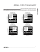
65Msps, 12-Bit, IF Sampling ADC SINGLE-TONE FFT PLOT (8192-POINT DATA RECORD) SINGLE-TONE FFT PLOT (8192-POINT DATA RECORD) -40 -50 -60 -70 HD2 HD3 -80 -30 -40 -50 -60 -70 HD2 HD3 -80 -90 -90 -100 -100 -110 -110 8 12 16 20 24 28 0 32 12 8 16 20 24 28 FREQUENCY (MHz) SINGLE-TONE FFT PLOT (8192-POINT DATA RECORD) SINGLE-TONE FFT PLOT (8192-POINT DATA RECORD) 0 fCLK = 65.000HMz fIN = 70.00671387MHz AIN = -0.494dBFS SNR = 68.33dBc SINAD = 68.27dBc THD = -86.91dBc SFDR = 89.
65Msps, 12-Bit, IF Sampling ADC Typical Operating Characteristics (continued) (VDD = 3.3V, OVDD = 2.0V, GND = 0, REFIN = REFOUT (internal reference), CREFOUT = 0.1µF, CL ≈ 5pF at digital outputs, differential input at -0.5dBFS, DCE = high, CLKTYP = high, PD = low, G/T = low, fCLK ≈ 65MHz (50% duty cycle), CREFP = CREFN = 0.1µF to GND, 1µF in parallel with 10µF between REFP and REFN, CCOM = 0.1µF in parallel with 2.2µF to GND, TA = +25°C, unless otherwise noted.
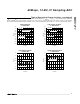
65Msps, 12-Bit, IF Sampling ADC SIGNAL-TO-NOISE RATIO vs. SAMPLING RATE SIGNAL-TO-NOISE + DISTORTION vs. SAMPLING RATE 69.0 DIFFERENTIAL CLOCK 69.0 SINAD (dB) 68.0 67.5 SINGLE-ENDED CLOCK 67.0 68.0 67.5 67.0 66.5 66.5 66.0 66.0 65.5 65.5 SINGLE-ENDED CLOCK 65.0 -70 35 40 45 50 55 60 65 70 30 35 40 45 50 55 60 65 fCLK (MHz) fCLK (MHz) TOTAL HARMONIC DISTORTION vs. SAMPLING RATE SPURIOUS-FREE DYNAMIC RANGE vs. SAMPLING RATE 100 MAX1211 toc11 30 fIN ≈ 32.
Typical Operating Characteristics (continued) (VDD = 3.3V, OVDD = 2.0V, GND = 0, REFIN = REFOUT (internal reference), CREFOUT = 0.1µF, CL ≈ 5pF at digital outputs, differential input at -0.5dBFS, DCE = high, CLKTYP = high, PD = low, G/T = low, fCLK ≈ 65MHz (50% duty cycle), CREFP = CREFN = 0.1µF to GND, 1µF in parallel with 10µF between REFP and REFN, CCOM = 0.1µF in parallel with 2.2µF to GND, TA = +25°C, unless otherwise noted.
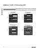
65Msps, 12-Bit, IF Sampling ADC SIGNAL-TO-NOISE RATIO vs. ANALOG INPUT FREQUENCY 69 68 69 68 67 SINAD (dB) 66 65 64 66 65 64 63 63 62 62 61 61 60 60 0 50 100 150 200 250 0 50 100 150 200 ANALOG INPUT FREQUENCY (MHz) ANALOG INPUT FREQUENCY (MHz) TOTAL HARMONIC DISTORTION vs. ANALOG INPUT FREQUENCY SPURIOUS-FREE DYNAMIC RANGE vs.
Typical Operating Characteristics (continued) (VDD = 3.3V, OVDD = 2.0V, GND = 0, REFIN = REFOUT (internal reference), CREFOUT = 0.1µF, CL ≈ 5pF at digital outputs, differential input at -0.5dBFS, DCE = high, CLKTYP = high, PD = low, G/T = low, fCLK ≈ 65MHz (50% duty cycle), CREFP = CREFN = 0.1µF to GND, 1µF in parallel with 10µF between REFP and REFN, CCOM = 0.1µF in parallel with 2.2µF to GND, TA = +25°C, unless otherwise noted.) SIGNAL-TO-NOISE RATIO vs.
65Msps, 12-Bit, IF Sampling ADC SIGNAL-TO-NOISE RATIO vs. CLOCK DUTY CYCLE 69 69 68 67 SINAD (dB) DCE = HIGH 66 65 DCE = LOW 64 67 DCE = HIGH 66 65 DCE = LOW 64 63 63 62 62 61 61 20 30 40 50 60 70 80 20 30 CLOCK DUTY CYCLE (%) 50 60 70 80 SPURIOUS-FREE DYNAMIC RANGE vs. CLOCK DUTY CYCLE TOTAL HARMONIC DISTORTION vs. CLOCK DUTY CYCLE 100 MAX1211 toc27 -65 -70 SINGLE-ENDED CLOCK fIN = 32.
Typical Operating Characteristics (continued) (VDD = 3.3V, OVDD = 2.0V, GND = 0, REFIN = REFOUT (internal reference), CREFOUT = 0.1µF, CL ≈ 5pF at digital outputs, differential input at -0.5dBFS, DCE = high, CLKTYP = high, PD = low, G/T = low, fCLK ≈ 65MHz (50% duty cycle), CREFP = CREFN = 0.1µF to GND, 1µF in parallel with 10µF between REFP and REFN, CCOM = 0.1µF in parallel with 2.2µF to GND, TA = +25°C, unless otherwise noted.) SIGNAL-TO-NOISE RATIO + DISTORTION vs.
65Msps, 12-Bit, IF Sampling ADC SIGNAL-TO-NOISE RATIO vs. TEMPERATURE 69.0 fIN ≈ 70MHz 69.5 69.0 68.5 68.5 68.0 SINAD (dB) 67.5 67.0 68.0 67.5 67.0 66.5 66.5 66.0 66.0 65.5 65.5 65.0 65.0 -70 -15 10 35 60 85 -40 -15 10 35 60 TEMPERATURE (°C) TEMPERATURE (°C) TOTAL HARMONIC DISTORTION vs. TEMPERATURE SPURIOUS-FREE DYNAMIC RANGE vs. TEMPERATURE 95 MAX1211 toc35 -40 fIN ≈ 70MHz -75 85 MAX1211 toc36 SNR (dB) MAX1211 toc34 fIN ≈ 70MHz 69.5 70.0 MAX1211 toc33 70.
Typical Operating Characteristics (continued) (VDD = 3.3V, OVDD = 2.0V, GND = 0, REFIN = REFOUT (internal reference), CREFOUT = 0.1µF, CL ≈ 5pF at digital outputs, differential input at -0.5dBFS, DCE = high, CLKTYP = high, PD = low, G/T = low, fCLK ≈ 65MHz (50% duty cycle), CREFP = CREFN = 0.1µF to GND, 1µF in parallel with 10µF between REFP and REFN, CCOM = 0.1µF in parallel with 2.2µF to GND, TA = +25°C, unless otherwise noted.) OFFSET ERROR vs. TEMPERATURE GAIN ERROR vs. TEMPERATURE VREF = 2.048V 0.
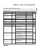
65Msps, 12-Bit, IF Sampling ADC PIN NAME FUNCTION 11 CLKTYP Clock Type Definition Input. Connect CLKTYP to GND to define the single-ended clock input. Connect CLKTYP to OVDD or VDD to define the differential clock input. 12–15, 36 VDD Analog Power Input. Connect VDD to a 3.0V to 3.6V power supply. Bypass VDD to GND with a parallel capacitor combination of ≥2.2µF and 0.1µF. Connect all VDD pins to the same potential. 17, 34 OVDD Output Driver Power Input. Connect OVDD to a 1.
MAX1211 65Msps, 12-Bit, IF Sampling ADC Detailed Description The MAX1211 uses a 10-stage, fully differential, pipelined architecture (Figure 1) that allows for highspeed conversion while minimizing power consumption. Samples taken at the inputs move progressively through the pipeline stages every half clock cycle. From input to output, the total clock-cycle latency is 8.5 clock cycles. Each pipeline converter stage converts its input voltage into a digital output code.
65Msps, 12-Bit, IF Sampling ADC Analog Inputs and Reference Configurations The MAX1211 full-scale analog input range is ±VREF with a common-mode input range of VDD / 2 ±0.8V. VREF is the difference between VREFP and VREFN. The MAX1211 provides three modes of reference operation. The voltage at REFIN (VREFIN) sets the reference operation mode (Table 1). To operate the MAX1211 with the internal reference, connect REFOUT to REFIN either with a direct short or through a resistive divider.
MAX1211 65Msps, 12-Bit, IF Sampling ADC Clock Duty-Cycle Equalizer (DCE) VDD S1H MAX1211 10kΩ CLKP 10kΩ DUTYCYCLE EQUALIZER S2H 10kΩ S1L The MAX1211 clock duty-cycle equalizer allows for a wide 20% to 80% clock duty cycle when enabled (DCE = OVDD or VDD). When disabled (DCE = GND), the MAX1211 accepts a narrow 45% to 65% clock duty cycle. See the Typical Operating Characteristics section for dynamic performance vs. clock duty-cycle plots.
65Msps, 12-Bit, IF Sampling ADC GRAY CODE OUTPUT CODE T = 1) (G/T BINARY D11 D0 TWO’S COMPLEMENT OUTPUT CODE T = 0) (G/T DECIMAL HEXADECIMAL EQUIVALENT EQUIVALENT DOR OF OF D11 D0 D11 D0 (CODE10) BINARY D11 D0 DECIMAL HEXADECIMAL EQUIVALENT EQUIVALENT DOR OF OF D11 D0 D11 D0 (CODE10) VINP - VINN VREFP = 2.162V VREFN = 1.138V ) ( 0x7FF +2047 >+1.0235V (DATA OUT OF RANGE) 0 0x7FF +2047 +1.0235V 0 0x7FE +2046 +1.0230V 0000 0000 0010 0 0x002 +2 +0.
Keep the capacitive load on DAV as low as possible (<25pF) to avoid large digital currents feeding back into the analog portion of the MAX1211 and degrading its dynamic performance. An external buffer on DAV isolates it from heavy capacitive loads. Refer to the MAX1211 evaluation kit schematic for an example of DAV driving back-end digital circuitry through an external buffer.
65Msps, 12-Bit, IF Sampling ADC GRAY-TO-BINARY CODE CONVERSION 1) THE MOST SIGNIFICANT BINARY BIT IS THE SAME AS THE MOST SIGNIFICANT GRAY-CODE BIT.
MAX1211 65Msps, 12-Bit, IF Sampling ADC Keep the capacitive load on the MAX1211 digital outputs D0–D11 as low as possible (<15pF) to avoid large digital currents feeding back into the analog portion of the MAX1211 and degrading its dynamic performance. The addition of external digital buffers on the digital outputs isolate the MAX1211 from heavy capacitive loads. To improve the dynamic performance of the MAX1211, add 220Ω resistors in series with the digital outputs close to the MAX1211.
65Msps, 12-Bit, IF Sampling ADC MAX1211 0Ω* INP 0.1µF 1 VIN N.C. T1 6 2 5 3 4 MINICIRCUITS ADT1-1WT 1 49.9Ω 0.5% N.C. 49.9Ω 0.5% T1 6 2 5 3 4 5.6pF 49.9Ω 0.5% N.C. 0.1µF MAX1211 COM 4.7µF 49.9Ω 0.5% MINICIRCUITS ADT1-1WT 0Ω* INN *0Ω RESISTORS CAN BE REPLACED WITH LOW-VALUE RESISTORS TO LIMIT THE INPUT BANDWIDTH. 5.6pF Figure 10.
MAX1211 65Msps, 12-Bit, IF Sampling ADC +3.3V 2.2µF 0.1µF VDD 39 1 2 16.2kΩ 3 *1µF MAX1211 MAX4250 5 MAX6062 1 0.1µF 0.1µF 0.1µF REFP REFIN REFN 2 0.1µF 1µF 4 3 2 10µF 6V 10µF 2.048V 47Ω 1 0.1µF 47µF 6V 38 REFOUT 0.1µF COM 3 0.1µF GND 2.2µF 1.47kΩ NOTE: ONE FRONT-END REFERENCE CIRCUIT PROVIDES ±15mA OF OUTPUT DRIVE. +3.3V 2.2µF 0.1µF VDD 39 REFIN REFP 1 0.1µF *1µF MAX1211 REFN 0.1µF 10µF 2 0.1µF 38 0.1µF REFOUT COM 3 GND 0.1µF 2.
13 12 11 4 14 1µF 3 MAX4254 1/4 0.1µF UNCOMMITTED *PLACE AS CLOSE TO THE DEVICE AS POSSIBLE. 1MΩ 1MΩ +3.3V 1 MAX6066 NOTE: ONE FRONT-END REFERENCE CIRCUIT SUPPORTS UP TO 8 MAX1211s. 0.1µF 2 2.500V 21.5kΩ 1% 21.5kΩ 1% 21.5kΩ 1% 21.5kΩ 1% 21.5kΩ 1% 9 10 6 5 2 3 10µF 6V 8 1/4 MAX4254 10µF 6V 7 1/4 MAX4254 10µF 6V 1 1/4 MAX4254 1.47kΩ 47Ω 1.47kΩ 47Ω 1.47kΩ 47Ω 330µF 6V 1.000V 330µF 6V 1.500V 330µF 6V 2.000V 2.2µF 10µF 2.2µF 10µF 0.1µF 0.1µF 0.1µF 0.
MAX1211 65Msps, 12-Bit, IF Sampling ADC Route high-speed digital signal traces away from the sensitive analog traces. Keep all signal lines short and free of 90° turns. Ensure that the differential analog input network layout is symmetric and that all parasitics are balanced equally. Refer to the MAX1211 evaluation kit data sheet for an example of symmetric input layout.
65Msps, 12-Bit, IF Sampling ADC Spurious-Free Dynamic Range (SFDR) SFDR is the ratio expressed in decibels of the RMS amplitude of the fundamental (maximum signal component) to the RMS value of the next-largest spurious component, excluding DC offset. Effective Number of Bits (ENOB) IM3 is the total power of the 3rd-order intermodulation products to the Nyquist frequency relative to the total input power of the two input tones f1 and f2. The individual input tone levels are at -7dBFS.
Package Information (The package drawing(s) in this data sheet may not reflect the most current specifications. For the latest package outline information, go to www.maxim-ic.com/packages.) QFN THIN 6x6x0.8.EPS MAX1211 65Msps, 12-Bit, IF Sampling ADC D2 D CL D/2 b D2/2 k E/2 E2/2 (NE-1) X e E CL E2 k e L (ND-1) X e e L CL CL L1 L L e A1 A2 e A PACKAGE OUTLINE 36, 40, 48L THIN QFN, 6x6x0.8mm 21-0141 E 1 2 NOTES: 1. DIMENSIONING & TOLERANCING CONFORM TO ASME Y14.5M-1994. 2.