
Owner manual


MAX1036–MAX1039
2.7V to 5.5V, Low-Power, 4-/12-Channel
2-Wire Serial 8-Bit ADCs
______________________________________________________________________________________ 19
External Reference
The external reference can range from 1.0V to V
DD
. For
maximum conversion accuracy, the reference must be
able to deliver up to 30µA and have an output imped-
ance of 1kΩ or less. If the reference has a higher output
impedance or is noisy, bypass it to GND as close to
AIN_/REF as possible with a 0.1µF capacitor.
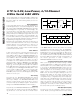
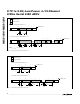
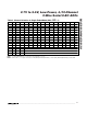
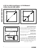
Transfer Functions
Output data coding for the MAX1036–MAX1039 is binary
in unipolar mode and two’s complement binary in bipolar
mode with 1LSB = (V
REF
/2
N
) where N is the number of
bits (8). Code transitions occur halfway between succes-
sive-integer LSB values. Figures 12 and 13 show the
input/output (I/O) transfer functions for unipolar and bi-
polar operations, respectively.
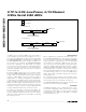
Layout, Grounding, and Bypassing
For best performance, use PC boards. Wire-wrap config-
urations are not recommended since the layout should
ensure proper separation of analog and digital traces. Do
not run analog and digital lines parallel to each other, and
do not lay out digital signal paths underneath the ADC
package. Use separate analog and digital PC board
ground sections with only one star point (Figure 14) con-
necting the two ground systems (analog and digital). For
lowest noise operation, ensure the ground return to the
star ground’s power supply is low impedance and as
short as possible. Route digital signals far away from sen-
sitive analog and reference inputs.
High-frequency noise in the power supply (V
DD
) could
influence the proper operation of the ADC’s fast
comparator. Bypass V
DD
to the star ground with a
0.1µF capacitor located as close as possible to the
MAX1036–MAX1039 power-supply pin. Minimize
capacitor lead length for best supply-noise rejection,
and add an attenuation resistor (5Ω) if the power sup-
ply is extremely noisy.
Definitions
Integral Nonlinearity
Integral nonlinearity (INL) is the deviation of the values
on an actual transfer function from a straight line. This
straight line can be either a best-straight-line fit or a line
drawn between the endpoints of the transfer function,
once offset and gain errors have been nullified. The INL
is measured using the endpoint method.
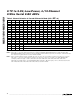
SCAN1 SCAN0 SCANNING CONFIGURATION
0 0 Scans up from AIN0 to the input selected by CS3–CS0 (default setting).
0 1 Converts the input selected by CS3–CS0 eight times.*
Scans up from AIN2 to the input selected by CS1 and CS0. When CS1 and CS0 are set for
AIN0–AIN2, the scanning stops at AIN2 (MAX1036/MAX1037).
10
Scans up from AIN6 to the input selected by CS3–CS0. When CS3–CS0 is set for AIN0–AIN6
scanning stops at AIN6 (MAX1038/MAX1039).
1 1 Converts the channel selected by CS3–CS0.*
Table 5. Scanning Configuration
*When operating in external clock mode, there is no difference between SCAN[1:0] = 01 and SCAN[1:0] = 11 and converting continues
until a not acknowledge occurs.
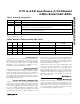
SEL2 SEL1 SEL0 REFERENCE VOLTAGE AIN_/REF
INTERNAL REFERENCE
STATE
00XV
DD
Analog input Always Off
0 1 X External reference Reference input Always Off
1 0 0 Internal reference Analog input Auto Shutdown
1 0 1 Internal reference Analog input Always On
1 1 X Internal reference Reference output Always On
Table 6. Reference Voltage and AIN_/REF Format
X = Don’t care.