
User guide

ISD5100 – SERIES
- 34 -
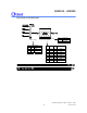
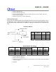
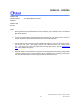
MI C+
MI C–
A
CAP
FTHRU
AGC
1 ( AG PD)
6 dB
To AutoMute
(Playback Only)
*
* Differential Path
AGC
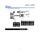
1514131211109876543210
VLS1 VLS0 VOL2 VOL1 VOL0 S1S1 S1S0 S1M1 S1M0 S2M1 S2M0 FLS0 FLD1 FLD0 FLPD AG PD
CFG1
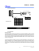
ANA IN (Analog Input)
The ANA IN pin is the analog input from the telephone chip set. It can be switched (by the I
2
C
interface) to the speaker output, the array input or to various other paths. This pin is designed to
accept a nominal 1.11 V p-p when at its minimum gain (6 dB) setting. There is additional gain
available, if required, in 3 dB steps, up to 15 dB. The gain settings are controlled from the I
2
C
interface.
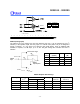
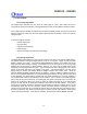
ANA IN Amplifier Gain Settings
AGPD CONDITION
0 Power Up
1 Power Down
MIC IN
Gain
Setting
Resistor Ratio
(Rb/Ra)
Gain Gain
2
(dB)
00 63.9 / 102 0.625 -4.1
01 77.9 / 88.1 0.883 -1.1
10 92.3 / 73.8 1.250 1.9
11 106 / 60 1.767 4.9
Note: Ra & Rb are in kΩ
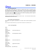
CFG0 Setting
(1)
0TLP Input
V
P-P
(3)
AIG1 AIG0
Gain
(2)
Array
In/Out V
P-P
Speaker
Out V
P-P
(4)
6 dB 1.110 0 0 0.625 0.694 2.22
9 dB 0.785 0 1 0.883 0.694 2.22
12 dB 0.555 1 0 1.250 0.694 2.22
15 dB 0.393 1 1 1.767 0.694 2.22
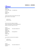
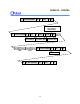
ANA IN
Input
ANA IN
Input Amplifier
NOTE:
f
CUTTOFF
2xR
a
C
COUP
1
R
a
R
b
C
COUP =
0.1
µ
F
Internal to the device