
Manual


ISD4004 Series
11
ISD
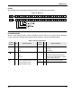
1. Stresses above those listed may cause permanent
damage to the device. Exposure to the absolute
maximum ratings may affect device reliability.
Functional operation is not implied at these conditions.
1. V
CC
= V
CCA
= V
CCD
2. V
SS
= V
SSA
= V
SSD
.
Table 8: Absolute Maximum Ratings (Die)
(1)
Condition Value
Junction temperature 150°C
Storage temperature range –65°C to +150°C
Voltage applied to any pad (V
SS
– 0.3 V) to
(V
CC
+ 0.3 V)
Voltage applied to MOSI, SCLK, INT,
RAC and SS pins (input current
limited to ± 20mA
(V
SS
– 1.0 V) to
5.5 V
V
CC
– V
SS
–0.3 V to +7.0 V
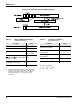
Table 9: Operating Conditions (Die)
Condition Value
Commercial operating
temperature range
0°C to +50°C
Supply voltage (V
CC
)
(1)
+2.7 V to +3.3 V
Ground voltage (V
SS
)
(2)
0 V
1. Typical values: T
A
= 25°C and 3.0 V.
2. All min/max limits are guaranteed by ISD via electrical testing or characterization. Not all specifications are
100 percent tested.
3. V
CCA
and V
CCD
connected together.
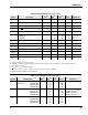
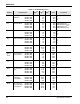
4. SS
= V
CCA
= V
CCD
, XCLK = MOSI = V
SSA
= V
SSD
and all other pins floating.
5. Measured with AutoMute feature disabled.
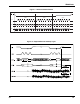
Table 10: DC Parameters (Die)
Symbol Parameters Min
(2)
Typ
(1)
Max
(2)
Units Conditions
V
IL
Input Low Voltage V
CC
x0.2 V
V
IH
Input High Voltage V
CC
x0.8 V
V
OL
Output Low Voltage 0.4 V I
OL
= 10 µA
V
OL1
RAC, INT Output Low Voltage 0.4 V I
OL
= 1 mA
V
OH
Output High Voltage V
CC
–0.4 V I
OH
= –10 µA
I
CC
V
CC
Current (Operating)
— Playback
— Record
15
25
30
40
mA
mA
R
EXT
= ¥
(3)
R
EXT
= ¥
(3)
I
SB
V
CC
Current (Standby) 1 10 µA
(3) (4)
I
IL
Input Leakage Current ±1 µA
I
HZ
MISO Tristate Current 1 10 µA
R
EXT
Output Load Impedance 5
K
W
R
ANA IN+
ANA IN+ Input Resistance 2.2 3.0 3.8
K
W
R
ANA IN–
ANA IN– Input Resistance 40 56 71
K
W
A
ARP
ANA IN+ or ANA IN– to AUDOUT Gain 25 dB
(5)