
Instruction Manual

ISD1916
Publication Release Date: September 11, 2007
- 18 - Revision 0
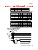
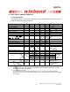
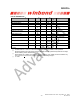
8. ELECTRICAL CHARACTERISTICS
8.1. DC PARAMETERS
After design is finalized, need Design engineering’s help to update the actual values on this DC
Parameter table and the timing parameters.
PARAMETER SYMBOL MIN
[2]
TYP
[1]
MAX
[2]
UNITS CONDITIONS
Input Low Voltage V
IL
0.3xVcc V
Input High Voltage V
IH
0.7xVcc V
Output Low Voltage V
OL
0.3xVcc V I
OL
= 4.0 mA
[3]
Output High Voltage V
OH
0.7xVcc V I
OH
= -1.6 mA
[3]
Standby Current I
STB
Y
1 10 µA
[4]
[5]
Record Current I
REC
20 30 mA V
CC
= 5.5V
[4]
[5]
Playback Current I
PLA
Y
20 30 mA V
CC
= 5.5V, no load
[4]
[5]
Pull-up device for REC , PlayE ,
PlayL , FT & M1 ~ M8 pins
R
PU1
600
kΩ
MIC+ Input Resistance R
MICP
18 KΩ
MIC- Input Resistance R
MICN
18 KΩ
AnaIn Input Resistance R
ANAIN
42 KΩ
MIC Differential Input V
IN1
15 300 mV Peak-to-peak
AnaIn Input V
IN2
1 V Peak-to-peak
Gain from MIC to SP+/- A
MSP
6 40 dB
V
IN
= 15~300 mVp-p,
AGC = 4.7 µF,
V
CC
= 2.4V~5.5V
Gain from AnaIn to SP+/- A
ASP
0 dB
V
CC
= 2.4V~5.5V
Output Load Impedance R
SPK
8 Ω Speaker load
Speaker Output Power Pout 670 mW
V
DD
= 5.5 V 1Vp-p,
1 kHz sine
wave at
AnaIn. R
SPK
= 8 Ω
313 mW
V
DD
= 4.4 V
117 mW
V
DD
= 3 V
49 mW
V
DD
= 2.4 V
Speaker Output Voltage V
OUT1
V
DD
V R
SPK
= 8Ω Speaker,
Typical buzzer
Total Harmonic Distortion THD 1 %
15 mV p-p 1 kHz sine
wave, Cmessage
weighted
Notes:
[1]
Typical values @ V
CC
= 5.5V, T
A
= 25° and sampling frequency (Fs) at 8 kHz, unless stated.
[2]
Not all specifications are 100 percent tested. All Min/Max limits are guaranteed by Winbond via design,
electrical testing and/or characterization.
[3]
LED output during recording.
[4]
V
CCA
, V
CCD
and V
CCP
are connected together. Also, V
SSA
, V
SSD
, V
SSP1
and V
SSP2
are linked together.
[5]
All required control pins must be at appropriate status. External components are biased under a separated
power supply.