
User guide


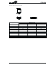

Absolute Maximum Ratings
Operating Temperature (Commercial) ........................................................................................................ 0°Cto70°C
Storage Temperature ............................................................................................................................ -50°Cto125°C
Applied VCC Voltage with Respect to VSS ............................................................................................... -0.3V to 6.0V
Applied Voltage on any Pin with Respect to VSS
........................................................................................................
-0.3V to V
CC
+0.3V
Note: These are stress ratings only. Stresses exceeding the range specified under ²Absolute Maximum Ratings² may
cause substantial damage to the device. Functional operation of this device at other conditions beyond those
listed in the specification is not implied and prolonged exposure to extreme conditions may affect device reliabil
-
ity.
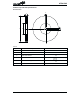
D.C. Characteristics
Ta=0°Cto70°C
Symbol Parameter
Test Conditions
Min. Typ. Max. Unit
V
CC
Conditions
V
CC
Operating Voltage
¾¾
2.2
¾
5.5 V
I
CC1
Operating Current 5V Read at 100kHz
¾¾
2mA
I
CC2
Operating Current 5V Write at 100kHz
¾¾
5mA
V
IL
Input Low Voltage
¾¾ -1 ¾
0.3V
CC
V
V
IH
Input High Voltage
¾¾
0.7V
CC
¾
V
CC
+0.5
V
V
OL
Output Low Voltage 2.4V
I
OL
=2.1mA
¾¾
0.4 V
I
LI
Input Leakage Current 5V
V
IN
=0 or V
CC
¾¾
1
mA
I
LO
Output Leakage Current 5V
V
OUT
=0 or V
CC
¾¾
1
mA
I
STB1
Standby Current 5V
V
IN
=0 or V
CC
¾¾
5
mA
I
STB2
Standby Current 2.4V
V
IN
=0 or V
CC
¾¾
4
mA
C
IN
Input Capacitance (See Note)
¾ f=1MHz 25°C ¾¾
6pF
C
OUT
Output Capacitance (See Note)
¾ f=1MHz 25°C ¾¾
8pF
Note: These parameters are periodically sampled but not 100% tested
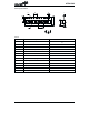
A.C. Characteristics
Ta=0°Cto70°C
Symbol Parameter Remark
Standard Mode*
V
CC
=5V±10%
Unit
Min. Max. Min. Max.
f
SK
Clock Frequency
¾¾
100
¾
400 kHz
t
HIGH
Clock High Time
¾
4000
¾
600
¾
ns
t
LOW
Clock Low Time
¾
4700
¾
1200
¾
ns
t
R
SDA and SCL Rise Time Note
¾
1000
¾
300 ns
t
F
SDA and SCL Fall Time Note
¾
300
¾
300 ns
t
HD:STA
START Condition Hold Time
After this period the first
clock pulse is generated
4000
¾
600
¾
ns
t
SU:STA
START Condition Setup Time
Only relevant for repeated
START condition
4000
¾
600
¾
ns
t
HD:DAT
Data Input Hold Time
¾
0
¾
0
¾
ns
t
SU:DAT
Data Input Setup Time
¾
200
¾
100
¾
ns
t
SU:STO
STOP Condition Setup Time
¾
4000
¾
600
¾
ns
HT24LC08
Rev. 1.20 2 November 4, 2002