
User Manual


HD44780U
8
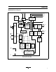
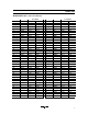
Pin Functions
Signal
No. of
Lines I/O
Device
Interfaced with Function
RS 1 I MPU Selects registers.
0: Instruction register (for write) Busy flag:
address counter (for read)
1: Data register (for write and read)
R/W 1 I MPU Selects read or write.
0: Write
1: Read
E 1 I MPU Starts data read/write.
DB4 to DB7
4 I/O MPU Four high order bidirectional tristate data bus
pins. Used for data transfer and receive between
the MPU and the HD44780U. DB7 can be used
as a busy flag.
DB0 to DB3 4 I/O MPU Four low order bidirectional tristate data bus pins.
Used for data transfer and receive between the
MPU and the HD44780U.
These pins are not used during 4-bit operation.
CL1 1 O Extension driver Clock to latch serial data D sent to the extension
driver
CL2 1 O Extension driver Clock to shift serial data D
M 1 O Extension driver Switch signal for converting the liquid crystal
drive waveform to AC
D 1 O Extension driver Character pattern data corresponding to each
segment signal
COM1 to COM16 16 O LCD Common signals that are not used are changed
to non-selection waveforms. COM9 to COM16
are non-selection waveforms at 1/8 duty factor
and COM12 to COM16 are non-selection
waveforms at 1/11 duty factor.
SEG1 to SEG40 40 O LCD Segment signals
V1 to V5 5 — Power supply Power supply for LCD drive
V
CC
–V5 = 11 V (max)
V
CC
, GND 2 — Power supply V
CC
: 2.7V to 5.5V, GND: 0V
OSC1, OSC2 2 — Oscillation
resistor clock
When crystal oscillation is performed, a resistor
must be connected externally. When the pin input
is an external clock, it must be input to OSC1.