
Instruction Manual
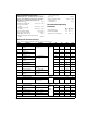


Function Select Table
MODE SELECTED DE0 DE1 RSEL
Receiver Zero ON, Driver Zero ON, Driver One OFF H L L
Receiver Zero ON, Driver Zero OFF, Driver One ON L H L
Receiver One ON, Driver Zero ON, Driver One OFF H L H
Receiver One ON, Driver Zero OFF, Driver One ON L H H
Receiver Zero ON, Driver Zero ON, Driver One ON H H L
Receiver One ON, Driver Zero ON, Driver One ON H H H
Driver Zero and Driver One TRI-STATE L L X
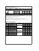
Truth Table for Receiver Zero
INPUTS OUTPUTS
DE0 RSEL (RI0+)–(RI0−) DO+ DO−
HL L LH
HL H HL
H L 100 mV
>
&
>
−100 mV X X
LX X ZZ
X = High or low logic state
Z = High impedance state
L = Low state
Truth Table for Receiver One
INPUTS OUTPUTS
DE1 RSEL (RI1+)–(RI1−) DO+ DO−
HH L LH
HH H HL
H H 100 mV
>
&
>
−100 mV X X
LX X ZZ
X = High or low logic state
Z = High impedance state
L = Low state
Truth Table for Current Drive
Driver Current Drive ISEL0 ISEL1
Driver 0 3.5 mA H X
Driver 0 8.5 mA L X
Driver 1 3.5 mA X H
Driver 1 8.5 mA X L
Applications Information
There are few common practices which should be employed
when designing PCB for Bus LVDS signaling. Recom-
mended practices are:
•
Use at least 4 PCB board layer (Bus LVDS signals,
ground, power and TTL signals).
•
Keep drivers and receivers as close to the (Bus LVDS
port side) connector as possible.
•
Bypass each Bus LVDS device and also use distributed
bulk capacitance. Surface mount capacitors placed close
to power and ground pins work best. Two or three multi-
layer ceramic (MLC) surface mount capacitors (0.1µ and
0.01 µF in parallel should be used between each V
CC
and
ground. The capacitors should be as close as possible to
the V
CC
pin.
•
Use controlled impedance traces which match the differ-
ential impedance of your transmission medium (i.e.,
Cable) and termination resistor.
•
Use the termination resistor which best matches the dif-
ferential impedance of your transmission line.
•
Leave unused Bus LVDS receiver inputs open (floating).
•
Isolate TTL signals from Bus LVDS signals.
MEDIA (CABLE, CONNECTOR OR BACKPLANE)
SELECTION:
•
Use controlled impedance media. The cables and con-
nectors should have a matched differential impedance.
•
Balanced cables (e.g., twisted pair) are usually better
than unbalanced cables (ribbon cable, simple coax) for
noise reduction and signal quality.
•
•
There are different types of failsafe situations to consider,
these are Open Input, Terminated Input, and other spe-
cial cases. The first, Open input failsafe occurs when only
one receiver is being used (R0 for example). The unused
receiver (R1) inputs should be left open for noise minimi-
zation. The second case is for terminated inputs. This oc-
curs when the inputs have a low impedance (typically 100
Ohm) termination (R
T
) across them, and the cable is un-
plugged. For this case, and if the output state needs to
maintain a known state, two external bias resistors may
be used to provide a strong common mode bias point.
For this a 10K Ohm pull up and pull down resistor may be
used to set the output high. Note that R
1
and R
2
should
be much larger ( 2 orders of magnitude) compared to R
T
to minimize loading effects to the Bus LVDS driver when
it is active.
www.national.com 6