
Instruction Manual
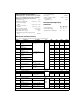


DC Electrical Characteristics (Continued)
T
A
= −40˚C to +85˚C unless otherwise noted, V
CC
= 3.3V
±
0.3V (Notes 2, 3)
Symbol Parameter Conditions Pin Min Typ Max Units
DEVICE CHARACTERISTICS
I
CCD
Power Supply Current No Load; DE = RSEL =
V
CC
Isel=0V
V
CC
25 45 mA
R
L
=27Ω; DE = RSEL
=V
CC
Isel=0V
24 40 mA
I
CCZ
DE = 0V; RSEL = V
CC
48mA
C
input
Capacitance at RO+/RO- 5 pF
C
output
Capacitance at DO+/DO- 5 pF
Note 1: “Absolute Maximum Ratings” are these beyond which the safety of the device cannot be guaranteed. They are not meant to imply that the device should
be operated at these limits. The table of “Electrical Characteristics” provides conditions for actual device operation.
Note 2: All currents into device pins are positive; all currents out of device pins are negative. All voltages are referenced to device ground unless otherwise specified.
Note 3: All typicals are given for V
CC
= +3.3V and T
A
= +25˚C, unless otherwise stated.
Note 4: ESD Rating: HBM (1.5 kΩ, 100 pF)
>
2 kV EIAJ (0Ω, 200 pF)
>
200V
Note 5: CL includes probe and fixture capacitance.
Note 6: Generator waveforms for all tests unless otherwise specified: f = 1MHz, ZO = 50Ω,t
f
=
<
6.0 ns (0
%
–100
%
).
Note 7: The DS92LV222A is a current mode device and only functions datasheet specifications when a resistive load is applied to the drivers outputs.
Note 8: During receiver select transition(s), data must be held in a steady state 15 ns before and 15 ns after the RSEL pin changes state.
Note 9: Channel-to-channel skew is the measurement between outputs of D0 and D1.
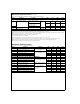
AC Electrical Characteristics
T
A
= −40˚C to +85˚C, V
CC
= 3.3V
±
0.3V (Note 6)
Symbol Parameter Conditions Min Typ Max Units
t
TLH
Transition Time Low to High R
L
=27Ω
Figures 2, 3
C
L
=10pF
Figures 2, 3
0.15 0.4 2.0 ns
t
THL
Transition Time High to Low 0.15 0.4 2.0 ns
t
PHZ
Disable Time High to Z R
L
=27Ω
Figures 4, 5
C
L
=10pF
Figures 4, 5
2.0 6.0 9.0 ns
t
PLZ
Disable Time Low to Z 2.0 6.0 9.0 ns
t
PZH
Enable Time Z to High 2.0 6.0 9.0 ns
t
PZL
Enable Time Z to Low 2.0 6.0 9.0 ns
DIFFERENTIAL RECEIVER TO DRIVER TIMING REQUIREMENTS
t
PHL_RD
Differential Prop. Delay High to Low R
L
=27Ω
Figures 2, 3
C
L
=10pF
Figures 2, 3
3.0 7.7 13 ns
t
PLH_RD
Differential Prop. Delay Low to High 3.0 8.0 13 ns
t
SK_RD
Pulse SKEW |t
PHL
–t
PLH
| 0 0.3 2.0 ns
t
PHL_RS0
Prop. Delay High to Low RSEL to Driver Outputs
R
L
=27Ω
Figures 6, 7
C
L
= 10 pF (Note 8)
2.0 7.5 13 ns
t
PLH_RS1
Prop. Delay Low to High 2.0 8.0 13 ns
t
PHL_R
0
D
x
Channel-to-Channel Skew R
0
to D
x
R
L
=27Ω
C
L
=10pF
(Note 9)
0.3 0.8 ns
t
PLH_R
0
D
x
Channel-to-Channel Skew R
0
to D
x
0.3 0.8 ns
t
PHL_R
1
D
x
Channel-to-Channel Skew R
1
to D
x
0.3 0.8 ns
t
PLH_R
1
D
x
Channel-to-Channel Skew R
1
to D
x
0.3 0.8 ns
3 www.national.com