
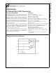
User guide
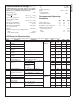


DC Electrical Characteristics (Continued)
Over recommended operating supply voltage and temperature ranges unless otherwise specified (Notes 2, 3)
Symbol Parameter Conditions Pin Min Typ Max Units
V
IH
Minimum Input High
Voltage
D
IN
, DE,
RE
2.0 V
CC
V
V
IL
Maximum Input Low
Voltage
GND 0.8 V
I
IH
Input High Current V
IN
=V
CC
or 2.4V −20
±
10 +20 µA
I
IL
Input Low Current V
IN
= GND or 0.4V −20
±
10 +20 µA
V
CL
Input Diode Clamp
Voltage
I
CLAMP
= −18 mA
−1.5 −0.8 V
I
CCD
Power Supply Current
Drivers Enabled,
Receivers Disabled
No Load, DE = RE = V
CC
,
DIN=V
CC
or GND
V
CC
55 80 mA
I
CCR
Power Supply Current
Drivers Disabled,
Receivers Enabled
DE=RE=0V,V
ID
=
±
300mV
73 80 mA
I
CCZ
Power Supply Current,
Drivers and Receivers
TRI-STATE
®
DE = 0V; RE = V
CC
,
DIN=V
CC
or GND 35 80 mA
I
CC
Power Supply Current,
Drivers and Receivers
Enabled
DE=V
CC
;RE=0V,
DIN=V
CC
or GND,
R
L
=27Ω
170 210 mA
I
OFF
Power Off Leakage
Current
V
CC
= 0V or OPEN,
D
IN
, DE, RE = 0V or OPEN,
V
APPLIED
= 3.6V (Port Pins)
DO+/RI+,
DO−/RI− −20 +20 µA
C
OUTPUT
Capacitance
@
Bus Pins DO+/RI+,
DO−/RI−
5pF
c
OUTPUT
Capacitance
@
R
OUT
R
OUT
7pF
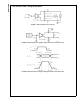
AC Electrical Characteristics
Over recommended operating supply voltage and temperature ranges unless otherwise specified (Note 6)
Symbol Parameter Conditions Min Typ Max Units
DIFFERENTIAL DRIVER TIMING REQUIREMENTS
t
PHLD
Differential Prop. Delay High to Low (Note 8) R
L
=27Ω,
Figures 2, 3
,
C
L
=10pF
0.6 1.4 2.2 ns
t
PLHD
Differential Prop. Delay Low to High (Note 8) 0.6 1.4 2.2 ns
t
SKD1
Differential Skew |t
PHLD
–t
PLHD
| (Note 9) 80 ps
t
SKD2
Chip to Chip Skew (Note 12) 1.6 ns
t
SKD3
Channel to Channel Skew (Note 13) 0.25 0.45 ns
t
TLH
Transition Time Low to High 0.6 1.2 ns
t
THL
Transition Time High to Low 0.5 1.2 ns
t
PHZ
Disable Time High to Z R
L
=27Ω,
Figures 4, 5
,
C
L
=10pF
38ns
t
PLZ
Disable Time Low to Z 38ns
t
PZH
Enable Time Z to High 38ns
t
PZL
Enable Time Z to Low 38ns
DIFFERENTIAL RECEIVER TIMING REQUIREMENTS
t
PHLD
Differential Prop. Delay High to Low (Note 8)
Figures 6, 7
,
C
L
=35pF
1.6 2.4 3.2 ns
t
PLHD
Differential Prop Delay Low to High (Note 8) 1.6 2.4 3.2 ns
t
SDK1
Differential Skew |t
PHLD
–t
PLHD
| (Note 9) 80 ps
t
SDK2
Chip to Chip Skew (Note 12) 1.6 ns
t
SDK3
Channel to Channel Skew (Note 13) 0.35 0.60 ns
t
TLH
Transition Time Low to High 1.5 2.5 ns
t
THL
Transition Time High to Low 1.5 2.5 ns
DS92LV090A
www.national.com 4