
Manual


DS31256
174 of 181
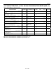
AC CHARACTERISTICS: PCI BUS INTERFACE
(V
DD
= 3.0V to 3.6V, T
A
= 0°C to +70°C.)
PARAMETER SYMBOL CONDITIONS MIN TYP MAX UNITS
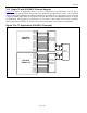
PCLK Period t1 (Note 15) 30 40 ns
PCLK Low Time t2 12 ns
PCLK High Time t3 12 ns
All PCI Inputs and I/O Setup Time to the
Rising Edge of PCLK
t4 7 ns
All PCI Inputs and I/O Hold Time from the
Rising Edge of PCLK
t5 (Note 16) 1 ns
Delay from the Rising Edge of PCLK to
Data Valid on all PCI Outputs and I/O
t6 2 11 ns
Delay from the Rising Edge of PCLK to
Three-state on all PCI Outputs and I/O
t7 28 ns
Delay from the Rising Edge of PCLK to
Active from Three-state on all PCI Outputs
and I/O
t8 2 ns
Note 15: Aggregate, maximum bandwidth and port speed for the DS31256 are directly proportional to PCLK frequency. Ensure that PCLK is
33MHz for maximum throughput.
Note 16: The PCI 2.1 Specification dictates that t5 should be 0ns. The 1ns value is noncompliance; however, this should not present an issue in
a real-world board design.
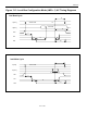
Figure 13-5. PCI Bus Interface AC Timing Diagram
PCLK
PCI In
p
ut
& I/O
PCI Out
p
ut
& I/O
PCI Out
p
ut &
I/O to Three-
State
PCI Out
p
ut &
I/O from Three-
State
Three-State
Three-State
t4 t5
t6
t7
t8
t1
t2 t3
Data Valid