
User Manual


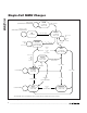


DS2710
Single-Cell NiMH Charger
2 _______________________________________________________________________________________2 _______________________________________________________________________________________
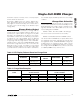
ABSOLUTE MAXIMUM RATINGS
RECOMMENDED DC OPERATING CONDITIONS
(4.0V ≤ V
DD
≤ 5.5V, T
A
= -20°C to +70°C.)
Stresses beyond those listed under “Absolute Maximum Ratings” may cause permanent damage to the device. These are stress ratings only, and functional
operation of the device at these or any other conditions beyond those indicated in the operational sections of the specifications is not implied. Exposure to
absolute maximum rating conditions for extended periods may affect device reliability.
Voltage Range on All Pins Relative to V
SS
............-0.3V to +6.0V
Continuous Source/Sink Current CS ...................................20mA
Continuous Source Current STATUS ..................................10mA
Operating Temperature Range ...........................-40°C to +85°C
Storage Temperature Range .............................-55°C to +125°C
Soldering Temperature...........................Refer to the IPC/JEDEC
J-STD-020 Specification.
PARAMETER SYMBOL CONDITIONS MIN TYP MAX UNITS
Supply Voltage V
DD
(Note 1) 4.0 5.5 V
Input Voltage Range CTEST, TMR, THM, VP1, VN1 -0.3 V
DD
V
DC ELECTRICAL CHARACTERISTICS
(4.0V ≤ V
DD
≤ 5.5V, T
A
= -20°C to +70°C, unless otherwise noted.)
PARAMETER SYMBOL CONDITIONS MIN TYP MAX UNITS
Supply Current, V
DD
I
DD
Operating mode (Note 2) 250 1000 μA
UVLO Threshold V
UVLO
V
DD
rising (Note 1) 3.5 3.9 V
UVLO Hysteresis V
UHYS
V
DD
falling from above V
UVLO
30 mV
Output-Voltage Low, CS V
OL1
V
DD
= 5.0V, I
OL
= +20mA (Note 1) 1.0 V
Output-Voltage High, CS V
OH1
V
DD
= 5.0V, I
OL
= -20mA (Note 1) 4.0 V
Output-Voltage Low, STATUS V
OL2
V
DD
= 5.0V, I
OL
= +2mA (Notes 1, 3) 0.50 V
Output-Voltage High, STATUS V
OH2
V
DD
= 5.0V, I
OH
= -2mA (Notes 1, 3) 4.0 V
Threshold Voltage,
-V Termination
V
-V
After t
THO
(Note 4) 1.0 2.0 3.0 mV
125 mV
Current-Sense Reference
Voltage
V
IREF
(Notes 1, 5)
-6 +6 %
Hysteresis, Current-Sense
Comparator
V
HYS-
COMP
Centered ~ 0.113V 18 23 27 mV
Propagation Time, Current-Sense
Comparator to Driver Output
t
PDLY
2mV overdrive/underdrive at trip threshold
(Notes 4, 6)
0.1 μs
CS Pin Pullup Current I
CS
V
DD
< V
UVLO
(Note 4) 2 10 μA
STATUS Pin Pulldown Current I
STAT
V
DD
< V
UVLO
(Note 4) 2 10 μA
Depleted Cell Voltage Threshold V
LOW
VP1 - VN1 0.9 1.0 1.1 V
Overcharge Voltage Threshold
V
MAX-
OPEN
VP1 - VN1, CS = high (Note 7) 1.55 1.65 1.75 V
Open Socket Voltage Threshold
V
MAX-
CHARGE
VP1 - VN1, CS = low (Note 7) 1.64 1.75 1.86 V
Offset, V
MAX-OPEN
- V
MAX-CHARGE
V
OS
(Note 7) 98 100 102 mV