
Manual


DS26519 16-Port T1/E1/J1 Transceiver
40 of 310
9.5 Global Resources
All 16 framers share a common microprocessor port and a common MCLK. There are two common software-
configurable BPCLK outputs (BPCLK[2:1]. A set of global registers includes global resets, global interrupt status,
interrupt masking, clock configuration, and the device ID register. See the global register bit map in
Table 10-7. A
common JTAG controller is used for all ports.
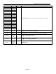
9.5.1 General-Purpose I/O Pins
The DS26519 has 16 GPIO pins (see GPIORR1 and GPIORR2). Each pin is assigned to one port and can be used
to output alarm status or be used as an input. GPIO[8:1] are globally controlled as a group, and GPIO[16:9] are a
second globally controlled group. Therefore, all GPIOs in a group output the same function.
Table 9-10 shows the
mux control of the GPIO pins.
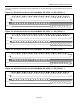
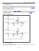
Figure 9-10. GPIO Mux Control
RLOFn
LOTCn
GTCR1.
RLOFLTC
A
LOSn
FLOSn
GTCR3.
LOSS
RSIGFn
GFCR1.
RLOSSFS
'0' '1'
GTCR1.
GPSEL[1:0]
GPIOn
GTCR1.
GPSEL2
GPIORR1.
bit (n-1)
RLOFm
LOTCm
GTCR2.
RLOFLTC
A
LOSm
FLOSm
GTCR4.
LOSS
RSIGFm
GFCR2.
RLOSSFS
'0' '1'
GTCR2.
GPSEL[1:0]
GPIOm
GTCR2.
GPSEL2
GPIORR2.
bit (m-1)
NOTE: n REFERS TO PORTS 1–8 AND m REFERS TO PORTS 9–16.
9.6 Per-Port Resources
Each port has an associated framer, LIU, BERT, jitter attenuator, and transmit/receive HDLC controller. Each of the
per-port functions has its own register space.