
Manual


DS26519 16-Port T1/E1/J1 Transceiver
138 of 310
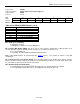
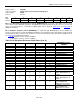
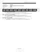
Register Name:
GTCCR2
Register Description:
Global Transceiver Clock Control Register 2
Register Address:
20F3h
Channels:
9 to 16
Bit # 7 6 5 4 3 2 1 0
Name
BPREFSEL3 BPREFSEL2 BPREFSEL1 BPREFSEL0 BFREQSEL — — —
Default 0 0 0 0 0 0 0 0
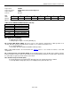
Bits 7 to 4: Backplane Clock Reference Selects (BPREFSEL[3:0]). These bits select which reference clock
source will be used for BPCLK2 generation. The BPCLK2 pin can be generated from the LIU’s 9 to 16 recovered
clocks, an external reference, or derivatives of MCLK input. This is shown in
Table 10-16. See Figure 9-9 for
additional information.
Bit 3: Backplane Frequency Select (BFREQSEL). In conjunction with BPRFSEL[3:0], this bit identifies the
reference clock frequency used by the DS26519 backplane clock generation circuit. Note that the setting of this bit
should match the T1E1 selection for the LIU whose recovered clock is being used to generate the backplane clock.
See
Figure 9-9 for additional information.
0 = Backplane reference clock is 2.048MHz.
1 = Backplane reference clock is 1.544MHz.
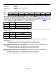
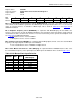
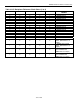
Table 10-16. Backplane Reference Clock Select (9 to 16)
BPREFSEL3 BPREFSEL2 BPREFSEL1 BPREFSEL0 BFREQSEL
REFERENCE CLOCK
SOURCE
0 0 0 0 0 2.048MHz RCLK9
0 0 0 0 1 1.544MHz RCLK9
0 0 0 1 0 2.048MHz RCLK10
0 0 0 1 1 1.544MHz RCLK10
0 0 1 0 0 2.048MHz RCLK11
0 0 1 0 1 1.544MHz RCLK11
0 0 1 1 0 2.048MHz RCLK12
0 0 1 1 1 1.544MHz RCLK12
0 1 0 0 0 2.048MHz RCLK13
0 1 0 0 1 1.544MHz RCLK13
0 1 0 1 0 2.048MHz RCLK14
0 1 0 1 1 1.544MHz RCLK14
0 1 1 0 0 2.048MHz RCLK15
0 1 1 0 1 1.544MHz RCLK15
0 1 1 1 0 2.048MHz RCLK16
0 1 1 1 1 1.544MHz RCLK16
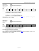
1 0 0 0 0
2.048MHz derived from
MCLK. (REFCLKIO is an
output.)
1 0 0 0 1
1.544MHz derived from
MCLK. (REFCLKIO is an
output.)
1 0 0 1 0
2.048MHz external clock
input at REFCLKIO.
(REFCLKIO is an input.)
1 0 0 1 1
1.544MHz external clock
input at REFCLKIO.
(REFCLKIO is an input.)