
User guide

DS2181A
041995 7/32
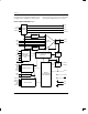
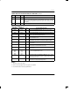
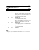
ACB: ADDRESS COMMAND BYTE Figure 2
(MSB) (LSB)
BM – – ADD3 ADD2 ADD1 ADD0 R/W
SYMBOL POSITION NAME AND DESCRIPTION
BM ACB.7 Burst Mode. If set (and ACB.1 through ACB.4 = 0), burst read or write is
enabled.
– ACB.6 Reserved; must be 0 for proper operation.
– ACB.5 Reserved; must be 0 for proper operation.
ADD3 ACB.4 MSB of register address.
ADD2 ACB.3
ADD1 ACB.2
ADD0 ACB.1 LSB of register address.
R/W ACB.0 Read/Write Select.
0 = Write address register.
1 = Read address register.
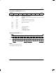
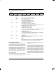
SERIAL PORT READ/WRITE Figure 3
CS
SCLK
SDI,SDO
ADDRESS/COMMAND DATA INPUT/OUTPUT
ADD0 ADD1 ADD2 ADD3 0 0 BM D0 D1 D2 D3 D4 D5 D6 D7R/W
NOTES:
1. SDI sampled on rising edge of SCLK.
2. SDO updated on falling edge of SCLK.