
User guide
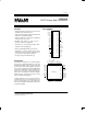

DS2181A
041995 5/32
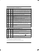
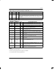
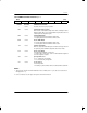
POWER AND TEST PIN DESCRIPTION (40–PIN DIP ONLY) Table 4
PIN SYMBOL TYPE DESCRIPTION
20 V
SS
– Signal Ground. 0.0 volts.
32 TEST I Test Mode. Tie to V
SS
to select the old DS2181 sync algorithm and to tri–
state the synchronizer status pins on the DS2181AQ. Tie to V
DD
to select the
new DS2181A sync algorithm and activate the synchronizer status pins on the
DS2181AQ.
40 V
DD
– Positive Supply. 5.0 volts.
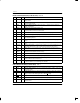
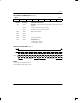
REGISTER SUMMARY Table 5
REGISTER ADDRESS T/R
1
DESCRIPTION/FUNCTION
RIMR 0000 R Receive Interrupt Mask Register. Allows masking of alarm
generated interrupts.
RSR 0001 R
2
Receive Status Register. Reports all receive alarm conditions.
BVCR 0010 R Bipolar Violation Count Register. 8-bit presettable counter
which records individual bipolar violations.
CECR 0011 R CRC4 Error Count Register. 8-bit presettable counter which
records individual errors.
FECR 0100 R Frame Error Count Register. 8-bit presettable counter which
logs individual errors in the received frame alignment signal.
RCR 0101 R Receive Control Register. Establishes receive side operating
characteristics.
CCR 0110 T/R Common Control Register. Establishes additional operating
characteristics for transmit and receive sides.
TCR 0111 T Transmit Control Register. Establishes transmit side operation
characteristics.
TIR1
TIR2
TIR3
TIR4
1000
1001
1010
1011
T Transmit Idle Registers. Designates which outgoing timeslots
are to be substituted with idle code.
TINR 1100 T Transmit International and National Register. When enabled
via the TCR, contents inserted into the outgoing national and/or
international bit positions.
TXR 1101 T Transmit Extra Register. When enabled via the TCR, contents
inserted into the out going extra bit positions.
NOTES:
1. Transmit or receive side register.
2. RSR is a read-only register; all other registers are read/write.
3. Reserved bit locations must be programmed to 0.