
User Manual
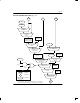

DS2153Q
022697 40/48
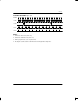
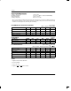
ABSOLUTE MAXIMUM RATINGS*
Voltage on Any Pin Relative to Ground –1.0V to +7.0V
Operating Temperature 0°C to 70°C
(–40°C to +85°C for DS2153QN)
Storage Temperature –55°C to +125°C
Soldering Temperature 260°C for 10 seconds
* This is a stress rating only and functional operation of the device at these or any other conditions above those
indicated in the operation sections of this specification is not implied. Exposure to absolute maximum rating
conditions for extended periods of time may affect reliability.
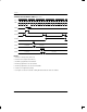
RECOMMENDED DC OPERATION CONDITIONS (0°C to 70°C)
(–40°C to +85°C for DS2153QN)
PARAMETER SYMBOL MIN TYP MAX UNITS NOTES
Logic 1 V
IH
2.0 V
DD
+0.3 V
Logic 0 V
IL
–0.3 +0.8 V
Supply for DS2153Q V
DD
4.75 5.25 V 1
Supply for DS2153QN V
DD
4.80 5.25 V 1
CAPACITANCE (t
A
=25°C)
PARAMETER SYMBOL MIN TYP MAX UNITS NOTES
Input Capacitance C
IN
5 pF
Output Capacitance C
OUT
7 pF
DC CHARACTERISTICS (0°C to 70°C; V
DD
=5V + 5%)
(–40°C to +85°C; V
DD
=5V +5%/–4% for DS2153QN)
PARAMETER SYMBOL MIN TYP MAX UNITS NOTES
Supply Current @ 5V I
DD
60 mA 2
Input Leakage I
IL
–1.0 +1.0 µA 3
Output Leakage I
LO
1.0 µA 4
Output Current (2.4V) I
OH
–1.0 mA
Output Current (0.4V) I
OL
+4.0 mA
NOTES:
1. Applies to RVDD, TVDD, and DVDD.
2. TCLK=2.048 MHz.
3. 0.0V < V
IN
< V
DD
.
4. Applies to INT1
and INT2 when 3–stated.