
User Manual

DS2153Q
022697 30/48
DS2153Q will divide the attached crystal by either 3.5 or
4.5 instead of the normal 4 to keep the buffer from over-
flowing. When the device divides by either 3.5 or 4.5, it
also sets the Jitter Attenuator Limit Trip (JALT) bit in the
Receive Information Register (RIR.5).
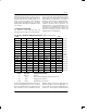
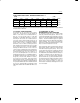
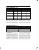
CRYSTAL SELECTION GUIDELINES Table 12–4
PARAMETER SPECIFICATION
Parallel Resonant Frequency 8.192 MHz
Mode Fundamental
Load Capacitance 18 pF to 20 pF (18.5 pF nominal)
Tolerance ±50 ppm
Pullability CL=10 pF, delta frequency=+175 to +250 ppm
CL=45 pF, delta frequency=–175 to –250 ppm
Effective Series Resistance 30 ohms maximum
Crystal Cut AT
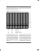
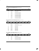
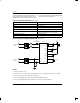
DS2153Q EXTERNAL ANALOG CONNECTIONS Figure 12–1
+5V
+
68 µF
0.1 µF
0.1 µF
0.1 µF
8.192 MHz
DVDD
DVSS
RVDD
RVSS
TVDD
TVSS
XTAL1
XTAL2
TTIP
TRING
RTIP
RRING
DS2153Q
0.1 µF
Rr Rr
1.15:1
E1 TRANSMIT
PAIR
E1 RECEIVE
LINE
0.47 µF
(NON–POLARIZED)
(OR 1.36:1)
1:1
Rt
Rt
0.01 µF
NOTES:
1. All resistor values are ±1%.
2. The Rt resistors are used to increase the transmitter return loss or to protect the device from over–voltage.
3. The Rr resistors are used to terminate the receive E1 line.
4. For 75 ohm termination, Rr=37.5 ohms/for 120 ohm termination Rr=60 ohms.
5. See the separate Application Note for details on how to construct a protected interface.