
User Manual

DS2153Q
022697 3/48
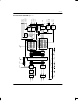
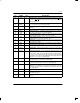
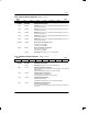
DS2153Q BLOCK DIAGRAM Figure 1–1
RCLK
RLINK
RLCLK
RCHBLK
RCHCLK
RSER
SYSCLK
RSYNC
TCLK
TSER
TSYNC
TCHCLK
TCHBLK
CS WR(R/W) RD(DS) ALE(AS) AD0 – AD7 INT1/INT2
RRING
RTIP
TRING
TTIP
ACLKI XTAL1 XTAL2 RLOS
XTAL/VCO/PLL
Filter
Peak
Detect
Clock/
Data
Recovery
Line
Drivers
Wave
Shaping
Parallel Control Port
(routed to all blocks)
32.768 MHz
Receive Side
Framer
Transmit Side Formatter
Sa Bit
Extraction
Timing
Control
Elastic
Store
mux
Loss of
clock
data
sync
Elastic
Store
Timing
Control
Sa
Insert
Logic
TLINK
TLCLK
BTS
TCLK Detect
Local Loopback
Jitter Attenuation Mux
(can be placed in either the transmit or receive paths)
Remote Loopback
Framer Loopback
AIS Generation
HDB3 Encode
CRC4 Generation
Idle Code Insertion
Signaling Insertion
Sa Bit Insertion
E Bit Insertion
Si Bit Insertion
FAS Word Insertion
HDB3 Decoder
BPV Counter
Synchronizer
Alarm Detection
CRC4 Error Count
E Bit Count
FAS Error Count
Signaling Extraction