
User Manual

DS2153Q
022697 27/48
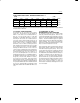
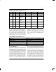
1 TAF.3 Frame Alignment Signal Bit.
0 TAF.2 Frame Alignment Signal Bit.
1 TAF.1 Frame Alignment Signal Bit.
1 TAF.0 Frame Alignment Signal Bit.
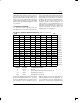
TNAF: TRANSMIT NON–ALIGN FRAME REGISTER (Address=21 Hex)
(MSB) (LSB)
Si 1 A Sa4 Sa5 Sa6 Sa7 Sa8
SYMBOL POSITION NAME AND DESCRIPTION
Si TNAF.7 International Bit.
1 TNAF.6 Frame Non–Alignment Signal Bit.
A TNAF.5 Remote Alarm.
Sa4 TNAF.4 Additional Bit 4.
Sa5 TNAF.3 Additional Bit 5.
Sa6 TNAF.2 Additional Bit 6.
Sa7 TNAF.1 Additional Bit 7.
Sa8 TNAF.0 Additional Bit 8.
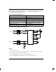
12.0 LINE INTERFACE FUNCTIONS
The line interface function in the DS2153Q contains
three sections; (1) the receiver which handles clock and
data recovery, (2) the transmitter which waveshapes
and drives the E1 line, and (3) the jitter attenuator. Each
of the these three sections is controlled by the Line Inter-
face Control Register (LICR) which is described below.
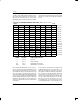
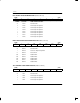
LICR: LINE INTERFACE CONTROL REGISTER (Address=18 Hex)
(MSB) (LSB)
L2 L1 L0 EGL JAS JABDS DJA TPD
SYMBOL POSITION NAME AND DESCRIPTION
LB2 LICR.7 Line Build Out Bit 2. Transmit waveshape setting; see Table 12.2.
LB1 LICR.6 Line Build Out Bit 1. Transmit waveshape setting; see Table 12.2.
LB0 LICR.5 Line Build Out Bit 0. Transmit waveshape setting; see Table 12.2.
EGL LICR.4 Receive Equalizer Gain Limit.
0 = –12 dB
1 = –30 dB
JAS LICR.3 Jitter Attenuator Select.
0=place the jitter attenuator on the receive side
1=place the jitter attenuator on the transmit side
JABDS LICR.2 Jitter Attenuator Buffer Depth Select .
0=128 bits
1=32 bits (use for delay sensitive applications)
LICR