
User Manual

DS2153Q
022697 10/48
TSA1 TCR1.2 Transmit Signaling All Ones.
0=normal operation
1=force timeslot 16 in every frame to all ones
TSM TCR1.1 TSYNC Mode Select.
0=frame mode (see the timing in Section 13)
1=CAS and CRC4 multiframe mode (see the timing in Section 13)
TSIO TCR1.0 TSYNC I/O Select.
0=TSYNC is an input
1=TSYNC is an output
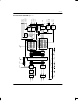
Note: See Figure 13–9 for more details about how the Transmit Control Registers affect the operation of the
DS2153Q.
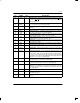
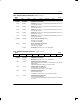
TCR2: TRANSMIT CONTROL REGISTER 2 (Address=13 Hex)
(MSB) (LSB)
Sa8S Sa7S Sa6S Sa5S Sa4S – AEBE P16F
SYMBOL POSITION NAME AND DESCRIPTION
Sa8S TCR2.7 Sa8 Bit Select. Set to one to source the Sa8 bit from the TLINK pin; set to
zero to not source the Sa8 bit.
Sa7S TCR2.6 Sa7 Bit Select. Set to one to source the Sa7 bit from the TLINK pin; set to
zero to not source the Sa7 bit.
Sa6S TCR2.5 Sa6 Bit Select. Set to one to source the Sa6 bit from the TLINK pin; set to
zero to not source the Sa6 bit.
Sa5S TCR2.4 Sa5 Bit Select. Set to one to source the Sa5 bit from the TLINK pin; set to
zero to not source the Sa5 bit.
Sa4S TCR2.3 Sa4 Bit Select. Set to one to source the Sa4 bit from the TLINK pin; set to
zero to not source the Sa4 bit.
– TCR2.2 Not Assigned. Should be set to zero when written.
AEBE TCR2.1 Automatic E–Bit Enable.
0=E–bits not automatically set in the transmit direction
1=E–bits automatically set in the transmit direction
P16F TCR2.0 Function of Pin 16.
0=Receive Loss of Sync (RLOS)
1=Loss of Transmit Clock (LOTC)
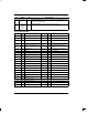
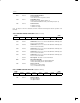
CCR1: COMMON CONTROL REGISTER 1 (Address=14 Hex)
(MSB) (LSB)
FLB
THDB3 TG802 TCRC4 RSM RHDB3 RG802 RCRC4
SYMBOL POSITION NAME AND DESCRIPTION
FLB CCR1.7 Framer Loopback.
0=loopback disabled
1=loopback enabled