
Owner manual

DS2151Q
022697 10/46
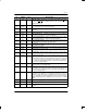
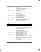
TLINK TCR1.2 TLINK Select. (see note below)
0=source FDL or Fs bits from TFDL register
1=source FDL or Fs bits from the TLINK pin
TBL TCR1.1 Transmit Blue Alarm. (see note below)
0=transmit data normally
1=transmit an unframed all one’s code at TPOS and TNEG
TYEL TCR1.0 Transmit Yellow Alarm. (see note below)
0=do not transmit yellow alarm
1=transmit yellow alarm
Note: for a detailed description of how the bits in TCR1 affect the transmit side formatter of the DS2151Q, please see
Figure 13–9.
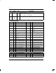
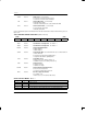
TCR2: TRANSMIT CONTROL REGISTER 2 (Address=36 Hex)
(MSB) (LSB)
TEST1 TEST0 TZBTSI TSDW TSM TSIO TD4YM B7ZS
SYMBOL POSITION NAME AND DESCRIPTION
TEST1 TCR2.7 Test Mode Bit 1 for Output Pins. See Table 3–1.
TEST0 TCR2.6 Test Mode Bit 0 for Output Pins. See Table 3–1.
TZBTSI TCR2.5 Transmit Side ZBTSI Enable.
0=ZBTSI disabled
1=ZBTSI enabled
TSDW TCR2.4 TSYNC Double–Wide. (note: this bit must be set to zero when TCR2.3=1
or when TCR2.2=0)
0=do not pulse double–wide in signaling frames
1=do pulse double–wide in signaling frames
TSM TCR2.3 TSYNC Mode Select.
0=frame mode (see the timing in Section 13)
1=multiframe mode (see the timing in Section 13)
TSIO TCR2.2 TSYNC I/O Select.
0=TSYNC is an input
1=TSYNC is an output
TD4YM TCR2.1 Transmit Side D4 Yellow Alarm Select.
0=zeros in bit 2 of all channels
1=a one in the S–bit position of frame 12
B7ZS TCR2.0 Bit 7 Zero Suppression Enable.
0=no stuffing occurs
1=Bit 7 force to a one in channels with all zeros
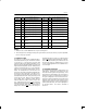
OUTPUT PIN TEST MODES Table 3–1
TEST1 TEST0 EFFECT ON OUTPUT PINS
0 0 operate normally
0 1 force all output pins 3–state (including all I/O pins and parallel port pins)
1 0 force all output pins low (including all I/O pins except parallel port pins)
1 1 force all output pins high (including all I/O pins except parallel port pins)