
Owner's manual


DS21455/DS21458 Quad T1/E1/J1 Transceivers
30 of 270
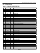
PIN NAME TYPE FUNCTION
B7 DVSS — Digital Signal Ground
B9 DVSS — Digital Signal Ground
H20 DVSS — Digital Signal Ground
L20 DVSS — Digital Signal Ground
N17 DVSS — Digital Signal Ground
J4 ESIBRD1 I/O Extended System Information Bus Read for Transceiver 1
C13 ESIBRD2 I/O Extended System Information Bus Read for Transceiver 2
C3 ESIBRD3 I/O Extended System Information Bus Read for Transceiver 3
U13 ESIBRD4 I/O Extended System Information Bus Read for Transceiver 4
W6 ESIBS0_1 I/O Extended System Information Bus 0 for Transceiver 1
F18 ESIBS0_2 I/O Extended System Information Bus 0 for Transceiver 2
D7 ESIBS0_3 I/O Extended System Information Bus 0 for Transceiver 3
T20 ESIBS0_4 I/O Extended System Information Bus 0 for Transceiver 4
V9 ESIBS1_1 I/O Extended System Information Bus 1 for Transceiver 1
B17 ESIBS1_2 I/O Extended System Information Bus 1 for Transceiver 2
A6 ESIBS1_3 I/O Extended System Information Bus 1 for Transceiver 3
J20 ESIBS1_4 I/O Extended System Information Bus 1 for Transceiver 4
U1
INT
O
Interrupt for All Four Transceivers
Y15 JTCLK I JTAG Clock
N1 JTDI I JTAG Data Input
V19 JTDO O JTAG Data Output
W13 JTMS I JTAG Test Mode Select
V18 JTRST I Jtag Reset
K2 LIUC/TPD I Line Interface Connect for All Four Transceivers or Transmit Power-Down Enable
T1 MCLK1 I Master Clock for Transceiver 1 and Transceiver 3
W20 MCLK2 I Master Clock for Transceiver 2 and Transceiver 4
U10 MUX I Mux Bus Select
M2 RCHBLK1 O Receive Channel Block for Transceiver 1
G17 RCHBLK2 O Receive Channel Block for Transceiver 2
G4 RCHBLK3 O Receive Channel Block for Transceiver 3
Y12 RCHBLK4 O Receive Channel Block for Transceiver 4
J1 RCHCLK1 O Receive Channel Clock for Transceiver 1
D14 RCHCLK2 O Receive Channel Clock for Transceiver 2
F3 RCHCLK3 O Receive Channel Clock for Transceiver 3
U14 RCHCLK4 O Receive Channel Clock for Transceiver 4
N3 RCLK1 O Receive Clock Output from the Framer on Transceiver 1
B13 RCLK2 O Receive Clock Output from the Framer on Transceiver 2
E3 RCLK3 O Receive Clock Output from the Framer on Transceiver 3
M18 RCLK4 O Receive Clock Output from the Framer on Transceiver 4
M4 RCLKI1 I Receive Clock Input for the LIU on Transceiver 1
A15 RCLKI2 I Receive Clock Input for the LIU on Transceiver 2
A4 RCLKI3 I Receive Clock Input for the LIU on Transceiver 3
R17 RCLKI4 I Receive Clock Input for the LIU on Transceiver 4
M3 RCLKO1 O Receive Clock Output from the LIU on Transceiver 1
C14 RCLKO2 O Receive Clock Output from the LIU on Transceiver 2
B4 RCLKO3 O Receive Clock Output from the LIU on Transceiver 3
T17 RCLKO4 O Receive Clock Output from the LIU On Transceiver 4
N2
RD (DS)
I Read Input (Data Strobe)
K4 RFSYNC1 O Receive Frame Sync (Before the Receive Elastic Store) for Transceiver 1
D17 RFSYNC2 O Receive Frame Sync (Before the Receive Elastic Store) for Transceiver 2
A2 RFSYNC3 O Receive Frame Sync (Before the Receive Elastic Store) for Transceiver 3
V14 RFSYNC4 O Receive Frame Sync (Before the Receive Elastic Store) for Transceiver 4
F1 RLCLK1 O Receive Link Clock for Transceiver 1