
Instruction Manual


______________________________________________________________________________________ 63
DS1876
SFP Controller with Dual LDD Interface
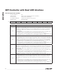
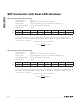
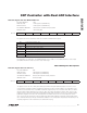
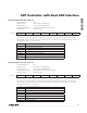
Table 02h, Register CEh–CFh: APC1 DAC
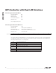
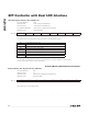
Table 02h, Register D0h–FFh: EMPTY
FACTORY DEFAULT 0000h
READ ACCESS PW2 or (PW1 and RWTBL2) or (PW1 and RTBL2)
WRITE ACCESS (PW2 and APC1EN = 0) or (PW1 and RWTBL2 and APC1EN = 0)
A2h AND B2h MEMORY Common A2h and B2h memory location
MEMORY TYPE Volatile
CEh 0 0 0 0 0 0 2
9
2
8
CFh 2
7
2
6
2
5
2
4
2
3
2
2
2
1
2
0
BIT 7 BIT 0
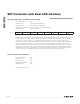
The digital value used for APC1 DAC. It is the result of LUT6 plus APC1 OFFSET times 4 recalled from Table
06h (Registers F8h–FFh) at the adjusted memory address found in TINDEX. This register is updated at the end
of the temperature conversion.
APC1 DAC = LUT6 + APC1 OFFSET x 4
REFIN
APC1
V
V APC1 DAC
1024
= ×
FACTORY DEFAULT 00h
READ ACCESS N/A
WRITE ACCESS N/A
A2h AND B2h MEMORY N/A
MEMORY TYPE None
These registers do not exist.