
Instruction Manual

______________________________________________________________________________________ 49
DS1876
SFP Controller with Dual LDD Interface
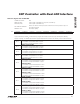
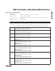
Table 02h, Register 8Ah: CNFGC
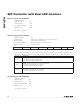
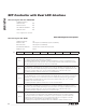
Table 02h, Register 8Bh: DEVICE ADDRESS
FACTORY DEFAULT 00h
READ ACCESS PW2 or (PW1 and RWTBL2) or (PW1 and RTBL2)
WRITE ACCESS PW2 or (PW1 and RWTBL2)
A2h AND B2h MEMORY Common A2h and B2h memory location
MEMORY TYPE Nonvolatile (SEE)
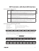
8Ah TXDFG2 TXDFLT2 TXDIO2 TXDFG1 TXDFLT1 TXDIO1 RESERVED RESERVED
BIT 7 BIT 0
BIT 7
TXDFG2: See Figure 9.
0 = FETG2, an internal signal, has no effect on TXDOUT2.
1 = FETG2 is enabled and ORed with other possible signals to create TXDOUT2.
BIT 6
TXDFLT2: See Figure 9.
0 = TXF2 pin has no effect on TXDOUT2.
1 = TXF2 pin is enabled and ORed with other possible signals to create TXDOUT2.
BIT 5
TXDIO2: See Figure 9.
0 = (default) TXD2 input signal is enabled and ORed with other possible signals to create TXDOUT2.
1 = TXD2 input signal has no effect on TXDOUT2.
BIT 4
TXDFG1: See Figure 9.
0 = FETG1, an internal signal, has no effect on TXDOUT1.
1 = FETG1 is enabled and ORed with other possible signals to create TXDOUT1.
BIT 3
TXDFLT1: See Figure 9.
0 = TXF1 pin has no effect on TXDOUT1.
1 = TXF1 pin is enabled and ORed with other possible signals to create TXDOUT1.
BIT 2
TXDIO1: See Figure 9.
0 = (default) TXD1 input signal is enabled and ORed with other possible signals to create TXDOUT1.
1 = TXD1 input signal has no effect on TXDOUT1.
BITS 1:0 RESERVED
FACTORY DEFAULT 00h
READ ACCESS PW2 or (PW1 and RWTBL2) or (PW1 and RTBL2)
WRITE ACCESS PW2 or (PW1 and RWTBL2)
A2h AND B2h MEMORY Common A2h and B2h memory location
MEMORY TYPE Nonvolatile (SEE)
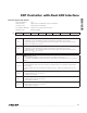
8Bh SEE SEE SEE SEE 2
3
2
2
2
1
SEE
BIT 7 BIT 0
This value becomes the I
2
C slave address for the main memory when the ASEL bit (Table 02h, Register 88h)
is set. If A0h is programmed to this register, the auxiliary memory is disabled. For example, writing xxxx_010x
makes the main device addresses A4h and B4h.