
Instruction Manual


DS1842A
76V, APD, Bias Output Stage with
Current Monitoring
_______________________________________________________________________________________ 5
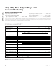
Pin Description
PIN NAME FUNCTION
1 MIR1 Current Mirror Monitor Output, 10:1 Ratio
2 MIR2 Current Mirror Monitor Output, 5:1 Ratio
3 GND
Ground Connection for Device. Connect directly to ground plane. Connect GND to PGND at a
single point. See the Layout Considerations section for more information.
4 FBOUT Feedback Output. Resistor-divider output.
5 CLAMP Clamp Input. Disables the current mirror output (MIROUT).
6 GATE FET Gate Connection
7 PGND
Source of Switch FET. Also connect to boost converter’s input and output capacitors. Connect
PGND to GND at a single point. See the Layout Considerations section for more information.
8 LX FET Drain Connection. Connect to switching inductor.
9, 10, 11 N.C. No Connection
12 FBIN Feedback Input. Resistor-divider input.
13 MIRIN Current Mirror Input
14 MIROUT Current Mirror Output. Connect to APD bias pin.
— EP Exposed Pad. Connect directly to the same ground plane as GND.
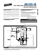
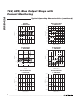
Block Diagram
TDFN
TOP VIEW
2
4
5
13
11
10
MIRIN
N.C.
N.C.
MIR2
FBOUT
CLAMP
1
14
MIROUTMIR1
3
12
FBINGND
6
9
N.C.GATE
7
8
LXPGND
DS1842A
*EP
*EXPOSED PAD.
+
DS1842A
LX
GATE
PGND
MIRIN
MIR1
CLAMP
MIROUT
CURRENT MIRROR
CURRENT
LIMIT
FBIN
MIR2
THERMAL
SHUTDOWN
FBOUT
R
1
R
2
GNDEP
Pin Configuration
Detailed Description
The DS1842A contains discrete high-voltage compo-
nents required to create an APD bias voltage and to
monitor the APD bias current. The device’s mirror out-
puts are a current that is a precise ratio of the output
current across a large dynamic range. The mirror
response time is fast enough to comply with GPON Rx
burst-mode monitoring requirements. The device has a
built-in current-limiting feature to protect APDs. The
APD current can also be shut down by CLAMP or ther-
mal shutdown. The internal FET and resistor-divider are
used in conjunction with a DC-DC boost controller to
precisely create the APD bias voltage.
Current Mirror
The DS1842A has two current mirror outputs. One is a
10:1 mirror connected at MIR1, and the other is a 5:1
mirror connected to MIR2.