
Owner's manual
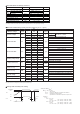


Absolute Maximum Ratings (Ta=25˚C)
Output
voltage
Nch open drain output
CMOS output
Power dissipation: VSOF5
Power dissipation: SOP4
Operating temperature range
Parameter Symbol Unit
VOUT
Pd
Pd
Topr
V
mW
mW
Storage temperature range
Tstg
Limits
– 40 ~ + 125
– 55 ~ + 125
210
CT pin input voltage
VCT
V
GND – 0.3 ~ VDD + 0.3
400
GND – 0.3 ~ + 7
GND – 0.3 ~ VDD + 0.3
˚C
˚C
Supply voltage
VDD – GND
– 0.3 ~ + 7
V
∗1
∗
2
Power dissipation: SSOP5
Pd
mW
540
∗3
Timing chart and delay time setting
∗4 All shipment is not inspected for design guarantee.
∗ Delay time setting (
tPLH
)
tPLH = τ × RCT × CCT(Sec)
-
Reference
-
τ :
RCT(Ω) :
CCT(F) :
Time constant
Designed to 10MΩ(Typ.) by resistance of the built-in IC
Capacitance of external capacitor
Capacitance of recommended CT capacitor is 100pF or more
VDET = 0.9V ~ 2.5V
Ta = 25°C
Ta =
-
25°C ~ 125°C
(min : 5.1E6, typ. : 6.0E6, max. : 6.9E6)
(min : 3.3E6, typ. : 6.0E6, max. : 8.7E6)
VDET = 2.6V ~ 4.8V
Ta = 25°C
Ta =
-
25°C ~ 125°C
(min : 5.9E6, typ. : 6.9E6, max. : 7.9E6)
(min : 3.8E6, typ. : 6.9E6, max. : 10.0E6)
( τ × RCT) :
Electrical characteristics (Unless otherwise noted; Ta=
-
25°C ~ +125°C)
VDET × 0.03 VDET × 0.05 VDET × 0.08
VDET × 0.03 VDET × 0.05 VDET × 0.07
µA
µA
µA
µA
IDD1
IDD2
Ileak
∆VDET
RL=470kΩ, VDD=L→H→L,
Ta=
-
40°C ~ +125°C
∗4
∗4
Temperature coefficient
of detection voltage
Hysteresis voltage
Circuit current ON
Circuit current OFF
Operating voltage range
"L" output current (Nch)
"H" output current (Pch)
(BU43XX series only)
Output leak current
(BU42XX series only)
VDET/∆T — ±30 — ppm/˚C
VDD=VDET
×
1.1, RL=470kΩ, Ta=25°C, VDET=0.9V~2.5V
VDD=VDET
×
1.1, RL=470kΩ, Ta=25°C, VDET=2.6V~4.8V
VDD=VDET+2.0V, VDET=0.9~1.3V
VDET=1.4~2.1V
VDET=2.2~2.7V
VDET=2.8~3.3V
VDET=3.4~4.2V
VDET=4.3~4.8V
V
V
VOPL
VOL 0.4V, Ta=25°C ~ 125°C
VDET 1.0V
VDET 1.1V
VOL 0.4V, Ta=
-
25°C ~ +25°C
VDD=VDS=7V, Ta=
-
40°C ~ +85°C
VDD=VDS=7V, Ta=+85°C ~ +125°C
mA
mA
IOH
VDS=0.5V, VDD=4.8V, VDET=0.9V~3.9V
VDS=0.5V, VDD=6.0V, VDET=4.0V~4.8V
IOL
9.0 10.0 11.0
— 0 1
— 0 0.1
— 1.40
— 1.58
— 1.75
— 1.93
— 2.10
—
0.30
VDD=VDET
-
0.2V, VDET=0.9~1.3V
— 0.880.15
VDET=1.4~2.1V
— 1.050.20
VDET=2.2~2.7V
— 1.230.25
VDET=2.8~3.3V
— 1.400.30
VDET=3.4~4.2V
— 1.580.35
VDET=4.3~4.8V
— 1.750.40
0.35
0.40
0.45
0.50
0.55 2.28
MΩRCTOutput delay resistance VDD=VDET
×
1.1, VCT=0.5V, Ta=25°C
5 40 —
1.7 3.4 —
VDS=0.05V, VDD=0.85V
20 100 —
VDS=0.5V, VDD=1.5V, VDET=1.7V~4.8V
1.0 3.3 —
0.9 — —
0.7 — —
VDS=0.5V, VDD=2.4V, VDET=2.7V~4.8V
4.0 7.2 —
2.0 4.0 —
µA
ICT
CT pin output current
VCT=0.1V, VDD=0.85V
VCT=0.5V, VDD=1.5V, VDET=1.7V~4.8V
200 400
—
VDD
×
0.35 VDD
×
0.45
VDD
×
0.55
VDD
×
0.40 VDD
×
0.50 VDD
×
0.60
VVCTH
CT pin
threshold voltage
Symbol Min. Max. Unit Conditions
Typ.
Parameter
VDD
VDD
VDET + ∆VDET
VDET
0V
VOH
VOUT
VOL
tPLH tPLHtPHL
∗1 Derating : 2.1mW/˚C for operation above Ta=25˚C PCB (70mmx70mm, t=1.6mm) glass epoxy mounting.
∗2 Derating : 4.0mW/˚C for operation above Ta=25˚C PCB (70mmx70mm, t=1.6mm) glass epoxy mounting.
∗3 Derating : 5.4mW/˚C for operation above Ta=25˚C PCB (70mmx70mm, t=1.6mm) glass epoxy mounting.
Note) This product is not designed for protection against radioactive rays.
<
=
>
=
<
=
<
=