
Instruction Manual

BR9010-W / F-W / FV-W / RFV-W / RFVM-W / BR9020-W / F-W / FV-W /
Memory IC
RFV-W / RFVM-W / BR9040-W / F-W / FV-W / RFV-W / RFVM-W
9/14
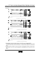
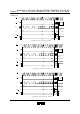
(3) Read Cycle
HIGH or LOW
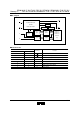
Fig.3 BR9010-W / F--W / FV-W / RFV-W / RFVM-W
1
4
81632
1
HIGH-Z
H
SK
CS
DI
DO
WC
L
H
L
H
L
01 10000
A0 A5 00
D0 D15 D15D0
HIGH-Z
STANDBY
t
CS
tOH
R / B
H
Read Data (n) Read Data (n+1)
HIGH or LOW
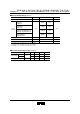
Fig.4 BR9020-W / F-W / FV-W / RFV-W / RFVM-W
1
4
8163248
1
HIGH-Z
H
SK
CS
DI
DO
R / B
WC
L
H
L
H
L
H
01 10000
A0 A6 0
D0
Read Data (n) Read Data (n+1)
D15 D15D0
HIGH-Z
STANDBY
t
CS
tOH
HIGH or LOW
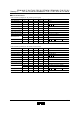
Fig.5 BR9040-W / F-W / FV-W / RFV-W / RFVM-W
1
4
81632
1
HIGH-Z
H
SK
CS
DI
DO
R / B
WC
L
H
L
H
L
H
01 10 000
A0 A6 A7
D0
Read Data (n) Read Data (n+1)
D15 D15D0
HIGH-Z
STANDBY
t
CS
tOH
1) On the falling edge of 16 th clock, the data stored in the specified address (n) is clocked out of the DO pin.
The Output DO is toggled after the internal propagation t
PDO
or
t
PD1
on the falling edge of SK. During t
PD0
or t
PD1,
the data
is the previous data or unstable, and to take in the data, t
PD
is needed. (Refer to Fig.1 Synchronous data input output
timing.)
2) The data stored in the next address is clocked out of the device on the falling edge of 32nd clock. The data stored in
the upper address every 16 clocks is output sequentially by the continual SK input. Also the read operation is reset by
CS High.