
Instruction Manual

BR9010-W / F-W / FV-W / RFV-W / RFVM-W / BR9020-W / F-W / FV-W /
Memory IC
RFV-W / RFVM-W / BR9040-W / F-W / FV-W / RFV-W / RFVM-W
7/14
z
zz
z
Operating
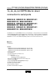
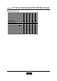
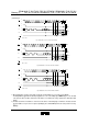
(1) Instruction Code
1010 1000
A0 A1 A2 A3 A4 A5 (
A6)
∗2
(A7)
∗1
A0 A1 A2 A3 A4 A5 (A6)
∗2
(A7)
∗1
1010 0100
1010 0011
∗ ∗ ∗ ∗ ∗ ∗ ∗ ∗
∗ ∗ ∗ ∗ ∗ ∗ ∗ ∗
D0 D1−D14 D15
(READ DATA)
D0 D1−D14 D15
(WRITE DATA)
1010 0000
READ
WRITE
Write Enable (WEN)
Write Disable (WDS)
Address and data must be transferred from LSB.
BR9020-W/F-W/FV-W/RFV-W/RFVM-W ∗1= "0"
BR9010-W/F-W/FV-W/RFV-W/RFVM-W ∗1, 2= "0"
Instruction
Start Bit Op Code
Address
Data
∗ Means either V
IH
or V
IL
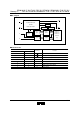
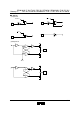
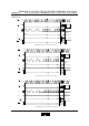
Synchronous Data Input Output Timing
CS
SK
DI
DO
WC
t
DIS
t
DIH
t
CSS
t
PD
t
OH
t
CSH
t
CS
t
PD
t
WL
t
WH
Input Data is clocked into the DI pin on the rising edge of the clock SK
Output data is clocked out on the falling edge of the SK clock.
The WC pin does not have any affect on the READ, WEN and WDS operations.
Between instructions, CS must be brought High for greater than the minimum of
t
CS
. If CS is maintained Low, the next instruction isn't detected.
Fig.1