
User guide

BR24L08-W / BR24L08F-W / BR24L08FJ-W
Memory ICs BR24L08FV-W / BR24L08FVM-W
18/25
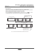
6) I / O circuit
• Pull up resister of SDA pin
The pull up resister is needed because SDA is NMOS open drain. Decide the value of this resister (R
PU) properly,
by considering V
IL, IL characteristics of a controller which control the device and VOH, IOL characteristics of the device.
If large R
PU is chosen, clock frequency need to be slow. In case of small RPU, the operating current increases.
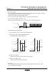
• Maximum of R
PU
Maximum of R
PU is determined by following factor.
c SDA rise time determined by R
PU and the capacitance of bus line (CBUS) must be less than TR.
And the other timing must keep the conditions of AC spec.
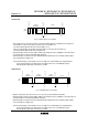
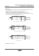
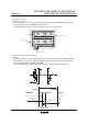
d When SDA bus is HIGH, the voltage A of SDA bus determined by a total input leak (I
L) of the all devices
connected to the bus and RPU must be enough higher than input HIGH level of a controller and the device,
including noise margin 0.2VCC.
A
IL IL
MICRO
COMPUTER
BR24LXX
SDA PIN
R
PU
THE CAPACITANCE OF
BUS LINE (CBUS)
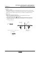
VCC − ILRPU − 0.2VCC ≥ VIH
RPU ≤
0.8VCC − VIH
IL
R
PU ≤
0.8×3−0.7×3
10×10
−6
≤ 300 [kΩ]
Examples : When V
CC=3V IL=10µA VIH=0.7VCC
According to
2