
Manual


BR24C21 / BR24C21F / BR24C21FJ / BR24C21FV
Memory ICs
!
!!
!Electrical characteristics (Unless otherwise noted, Ta=−40∼85°C, V
CC
=2.5∼5.5V)
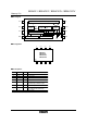
Parameter Symbol Min. Typ. Max. Unit Conditions
V
IH1
−−
V
V
IL1
−−
0.3V
CC V
V
OL
−−
0.4 V
Input leakage current I
LI
−
1 µA
SCL, VCLK, VIN=0V~VCC
Output leakage current ILO
−1
−1 −
1 µA
Operating current I
CC
−
3.0 mA
Standby current
I
SB
−
−
10 100
µA
0.7V
CC
SCL, SDA
SCL, SDA
SDA, I
OL=3.0mA
V
CC=5.5V, fSCL=400kHz
SDA, V
OUT=0V~VCC
"HIGH" input volatge1
"LOW" input volatge1
V
IH2
−−
V
V
IL2
−−
0.8 V
2.0
VCLK, VCC≥4.0V
VCLK
"HIGH" input volatge2
"LOW" input volatge2
V
IL3
−−
0.2V
CC V
VCLK, VCC<4.0V
"LOW" input volatge3
"LOW" output volatge
V
CC=5.5V, SDA=SCL=VCC, VCLK=GND
∗1
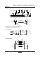
∗1 Transmit-Only Mode…After the power is on, the BR24C21, BR24C21F, BR24C21FJ and BR24C21FV are in Standby state without providing the clock on the VCLK pin.
After the VCLK pin is provided the clock, the device is switched from Standby to Transmit-Only Mode, and the operating current runs.
Bi-directional Mode…The BR24C21, BR24C21F, BR24C21FJ and BR24C21FV are in Standby state after each command is porformed.
!
!!
!
Operating timing characteristics
(Unless otherwise noted, Ta=−40∼85°C, V
CC
=2.5∼5.5V)
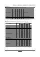
Parameter Symbol
Fast-mode
Vcc=2.5~5.5V
Standard-mode
Vcc=2.5~5.5V
Unit
f
SCL
kHz
t
HIGH
Noise erase valid time (SCL and SDA) t
I
µs
Data clock "HIGH" time
SCL frequency
µs
Data clock "LOW" time t
LOW
µs
SDA/SCL rise time t
R
µs
SDA/SCL fall time t
F
µs
Start condition hold time
tHD : STA
µs
Start condition setup time
tSU : STA
µs
Input data hold time
tHD : DAT
ns
Input data setup time
tSU : DAT
ns
Output data delay time (SCL) t
PD
µs
Stop condition setup time
tSU : STO
µs
Bus open time before start or transfer t
BUF
µs
t
WR
Min.
−
0.6
−
1.3
−
−
0.6
0.6
0
100
−
0.6
1.3
−
Typ.
−
−
−
−
−
−
−
−
−
−
−
−
−
−
Max.
400
−
0.1
−
0.3
0.3
−
−
−
−
0.9
−
−
10
Min.
−
4.0
−
4.7
−
−
4.0
4.7
0
250
−
4.0
4.7
−
Typ.
−
−
−
−
−
−
−
−
−
−
−
−
−
−
Max.
100
−
t
VHIGH
VCLK
"HIGH" time
µs
0.6
−−
4.0
−−
0.1
−
1.0
0.3
−
−
−
−
3.5
Output data delay time (VCLK) t
VPD
µs
−
−
1.0 −
−
2.0
−
−
10 msInternal write cycle time
Noise erase valid time (VCLK) t
VI
µs
<Transmit-Only Mode>
VCLK
"LOW" time t
VLOW
µs
Transmit-Only powerup time t
VPU
µs
VCLK hold time t
VHD
µs
VCLK setup time t
VSU
µs
−
1.3
0
0.6
0
−
−
−
−
−
0.1
−
−
−
−
−
4.7
0
4.0
0
−
−
−
−
−
0.1
−
−
Mode transition time t
VHZ
µs
−
− 0.5
−
− 1.0
−
−