
User guide

2
Standard ICs BA4560 / BA4560F / BA4560N
•
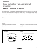
Internal circuit configuration
VCC
VEE
R2
R3
R1
Q5
Q1
– IN
+ IN
Q
2
Q6
Q9
Q8
Q4Q3
R4
Q10
Q7
Q11
R9
D
Q
13
R5
R6
R7
Q12 Q14
Q15
R8
OUT
•
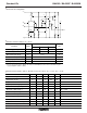
Absolute maximum ratings (Ta = 25°C)
Parameter Symbol
Limits
Unit
BA4560 BA4560F BA4560N
Power supply voltage V
CC ± 18 ± 18 ± 18 V
Power dissipation 800
∗
550
∗
900
∗
mW
Differential input voltage V
ID ± VCC V
Common-mode input voltage V
I V
Operating temperature Topr °C
Storage temperature Tstg °C
– 40 ~ + 85
– 55 ~ + 125
Pd
∗
Refer to the Pd characteristics diagram. The values for the BA4560F are those when it is mounted on a glass
epoxy PCB (50mm × 50mm × 1.6mm).
– VCC ~ VCC
•
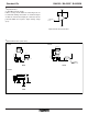
Electrical characteristics (unless otherwise noted, Ta = 25°C, VCC = +15 V, VEE = -15 V)
Parameter Symbol Min. Typ. Max. Unit Conditions
Input offset voltage V
IO — 0.5 6.0 mV RS ⬉ 10kΩ
Input offset current I
IO — 5 200 nA
Input bias current I
B — 50 500 nA
High-amplitude voltage gain A
V 86 100 — dB RL ⭌ 2kΩ, VO = ± 10V
Common-mode input voltage V
ICM ± 12 ± 14 — V
Maximum output voltage 1 V
OM1 ± 12 ± 14 — V RL ⭌ 10kΩ
Maximum output voltage 2 V
OM2 ± 10 ± 13 — V RL ⭌ 2kΩ
Common-mode rejection ratio CMRR 70 90 — dB R
S ⬉ 10kΩ
Power supply voltage rejection ratio PSRR — 30 150 R
S ⬉ 10kΩ
Slew rate S. R. — 4.0 — V /
µsA
V = 1, RL = 2kΩ
Input conversion noise voltage Vn — — 2.2
µV
Gain band width product GBW — 10 — MHz
µV / V
f = 10kHz