
Manual


5
4890AS–GPS–09/05
ATR0621 [Preliminary]
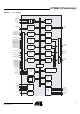
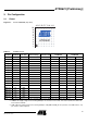
3. Pin Configuration
3.1 Pinout
Figure 3-1. Pinout LFBGA100 (Top View)
ATR0621
1
2
3
4
5
6
7
8
9
10
ABCDEFGHJK
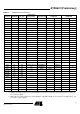
Table 3-1. ATR0621 Pinout
Pin Name LFBGA100 Pin Type
Pull Resistor
(Reset Value)
(1)
Firmware Label PIO Bank A PIO Bank B
CLK23 G9 IN
DBG_EN H4 IN PD
EM_A1 A6 OUT
EM_A2 A5 OUT
EM_A3 A4 OUT
EM_A4 A2 OUT
EM_A5 A3 OUT
EM_A6 B5 OUT
EM_A7 B4 OUT
EM_A8 B2 OUT
EM_A9 D4 OUT
EM_A10 C2 OUT
EM_A11 D6 OUT
EM_A12 D7 OUT
EM_A13 C3 OUT
EM_A14 C1 OUT
EM_A15 D5 OUT
EM_A16 C6 OUT
EM_A17 F8 OUT
Notes: 1. PD = internal pull-down resistor, PU = internal pull-up resistor, OH = switched to Output High at reset
2. VDDIO is the supply voltage for the following GPIO pins: P1, P2, P8, P12, P14, P16, P17, P18, P19, P20, P21, P23, P24,
P25, P26, P27 and P29
3. VDD_USB is the supply voltage for the following USB pins: USB_DM and USB_DP. For operation of the USB interface, sup-
ply of 3.0V to 3.6V is required.