Features • High Performance, Low Power AVR® 8-bit Microcontroller • Advanced RISC Architecture • • • • • • • • • • • – 124 Powerful Instructions - Most Single Clock Cycle Execution – 32 x 8 General Purpose Working Registers – Fully Static Operation – Up to 4 MIPS Throughput at 4 MHz Nonvolatile Program and Data Memories – 4K/8K Bytes of In-System Self-Programmable Flash (ATmega4HVD/8HVD) – 256 Bytes EEPROM – 512 Bytes Internal SRAM – Write/Erase Cycles: 10,000 Flash/ 100,000 EEPROM – Data Retention: 2
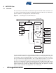
1. Pin Configurations Figure 1-1. Dual Row DFN/ MLF-pinout ATmega4HVD/8HVD. Top view Bottom view B10 B1 B9 B2 B8 B3 A1 A8 A7 A2 A6 A3 B4 B7 A4 A5 B5 B6 Table 1-1. Dual Row DFN/ MLF-pinout ATmega4HVD/8HVD.
ATmega4HVD/8HVD 1.1 1.1.1 Pin Descriptions VFET Input to the internal voltage regulator. 1.1.2 VCC Pin for connection of external decoupling capacitor. VCC is internally connected to the voltage regulator output VREG. 1.1.3 VREG Output from the internal voltage regulator. Internally connected to VCC. 1.1.4 GND Ground 1.1.5 Port B (PB2:PB0) Port B is a low-voltage 3-bit bi-directional I/O port with internal pull-up resistors (selected for each bit).
2. Overview The ATmega4HVD/8HVD is a monitoring and protection circuit for 1-cell Li-ion applications with focus on high security/authentication, low cost and high utilization of the cell energy. The device contains secure authentication features as well as autonomous battery protection during charging and discharging. The External Protection Input can be used to implement other battery protection mechanisms using external components, e.g.
ATmega4HVD/8HVD tains a high-voltage tolerant, open-drain IO pin that supports serial communication.
. AVR CPU Core 6.1 Overview This section discusses the AVR core architecture in general. The main function of the CPU core is to ensure correct program execution. The CPU must therefore be able to access memories, perform calculations, control peripherals, and handle interrupts. Figure 6-1.
ATmega4HVD/8HVD Six of the 32 registers can be used as three 16-bit indirect address register pointers for Data Space addressing – enabling efficient address calculations. One of the these address pointers can also be used as an address pointer for look up tables in Flash program memory. These added function registers are the 16-bit X-, Y-, and Z-register, described later in this section. The ALU supports arithmetic and logic operations between registers or between a constant and a register.
6.3.1 SREG – AVR Status Register Bit 7 6 5 4 3 2 1 0 I T H S V N Z C Read/Write R/W R/W R/W R/W R/W R/W R/W R/W Initial Value 0 0 0 0 0 0 0 0 SREG • Bit 7 – I: Global Interrupt Enable The Global Interrupt Enable bit must be set for the interrupts to be enabled. The individual interrupt enable control is then performed in separate control registers.
ATmega4HVD/8HVD 6.4 General Purpose Register File The Register File is optimized for the AVR Enhanced RISC instruction set.
Figure 6-3. The X-, Y-, and Z-registers 15 X-register XH XL 7 0 R27 (0x1B) 15 Y-register 0 R26 (0x1A) YH YL 7 0 R29 (0x1D) Z-register 0 7 0 7 0 R28 (0x1C) 15 ZH 7 0 ZL 0 7 R31 (0x1F) 0 R30 (0x1E) In the different addressing modes these address registers have functions as fixed displacement, automatic increment, and automatic decrement (see the instruction set reference for details). 6.
ATmega4HVD/8HVD 6.6 Instruction Execution Timing This section describes the general access timing concepts for instruction execution. The AVR CPU is driven by the CPU clock clkCPU, directly generated from the selected clock source for the chip. No internal clock division is used. Figure 6-4 shows the parallel instruction fetches and instruction executions enabled by the Harvard architecture and the fast-access Register File concept.
When an interrupt occurs, the Global Interrupt Enable I-bit is cleared and all interrupts are disabled. The user software can write logic one to the I-bit to enable nested interrupts. All enabled interrupts can then interrupt the current interrupt routine. The I-bit is automatically set when a Return from Interrupt instruction – RETI – is executed. There are basically two types of interrupts. The first type is triggered by an event that sets the interrupt flag.
ATmega4HVD/8HVD When using the SEI instruction to enable interrupts, the instruction following SEI will be executed before any pending interrupts, as shown in this example. Assembly Code Example sei ; set Global Interrupt Enable sleep; enter sleep, waiting for interrupt ; note: will enter sleep before any pending ; interrupt(s) C Code Example _SEI(); /* set Global Interrupt Enable */ _SLEEP(); /* enter sleep, waiting for interrupt */ /* note: will enter sleep before any pending interrupt(s) */ 6.7.
7. AVR Memories 7.1 Overview This section describes the different memories in the ATmega4HVD/8HVD. The AVR architecture has two main memory spaces, the Data Memory and the Program Memory space. In addition, the ATmega4HVD/8HVD features an EEPROM Memory for data storage. All three memory spaces are linear and regular. 7.2 In-System Reprogrammable Flash Program Memory The ATmega4HVD/8HVD contains 4/8K bytes On-chip In-System Reprogrammable Flash memory for program storage.
ATmega4HVD/8HVD 7.3 SRAM Data Memory Figure 7-2 shows how the ATmega4HVD/8HVD SRAM Memory is organized. The ATmega4HVD/8HVD is a complex microcontroller with more peripheral units than can be supported within the 64 locations reserved in the Opcode for the IN and OUT instructions. For the Extended I/O space from 0x60 - 0xFF in SRAM, only the ST/STS/STD and LD/LDS/LDD instructions can be used.
Figure 1. On-chip Data SRAM Access Cycles T1 T2 T3 clkCPU Address Compute Address Address valid Write Data WR Read Data RD Memory Access Instruction 7.4 Next Instruction EEPROM Data Memory The ATmega4HVD/8HVD contains 256 bytes of data EEPROM memory. It is organized as a separate data space, in which single bytes can be read and written. The EEPROM has an endurance of at least 100,000 write/erase cycles.
ATmega4HVD/8HVD tions. Refer to the instruction set section for more details. When using the I/O specific commands IN and OUT, the I/O addresses 0x00 - 0x3F must be used. When addressing I/O Registers as data space using LD and ST instructions, 0x20 must be added to these addresses. The ATmega4HVD/8HVD is a complex microcontroller with more peripheral units than can be supported within the 64 location reserved in Opcode for the IN and OUT instructions.
7.6.3 EECR – The EEPROM Control Register Bit 7 6 5 4 3 2 1 0 – – EEPM1 EEPM0 EERIE EEMPE EEPE EERE Read/Write R R R/W R/W R/W R/W R/W R/W Initial Value 0 0 X X 0 0 X 0 EECR • Bits 7:6 – Res: Reserved Bits These bits are reserved bits in the ATmega4HVD/8HVD and will always read as zero. • Bits 5, 4 – EEPM1 and EEPM0: EEPROM Programming Mode Bits The EEPROM Programming mode bit setting defines which programming action that will be triggered when writing EEPE.
ATmega4HVD/8HVD 4. Write a logical one to the EEMPE bit while writing a zero to EEPE in EECR. 5. Within four clock cycles after setting EEMPE, write a logical one to EEPE. Caution: An interrupt between step 4 and step 5 will make the write cycle fail, since the EEPROM Master Write Enable will timeout. If an interrupt routine accessing the EEPROM is interrupting another EEPROM access, the EEARL or EEDR Register will be modified, causing the interrupted EEPROM access to fail.
Assembly Code Example EEPROM_write: ; Wait for completion of previous write sbic EECR,EEWE rjmp EEPROM_write ; Set up address (r17) in address register out EEARL, r17 ; Write data (r16) to data register out EEDR,r16 ; Write logical one to EEMWE sbi EECR,EEMWE ; Start eeprom write by setting EEWE sbi EECR,EEWE ret C Code Example void EEPROM_write(unsigned int uiAddress, unsigned char ucData) { /* Wait for completion of previous write */ while(EECR & (1<
ATmega4HVD/8HVD The next code examples show assembly and C functions for reading the EEPROM. The examples assume that interrupts are controlled so that no interrupts will occur during execution of these functions.
8. System Clock and Clock Options 8.1 Clock Systems and their Distribution Figure 8-1 presents the principal clock systems in the AVR and their distribution. All of the clocks need not be active at a given time. In order to reduce power consumption, the clocks to modules not being used can be halted by using different sleep modes, as described in ”Power Management and Sleep Modes” on page 32. The clock systems are detailed below. Figure 8-1.
ATmega4HVD/8HVD ADC. The dedicated ADC clock allows halting the CPU and I/O clocks in order to reduce noise generated by digital circuitry. This gives more accurate ADC conversion results. 8.1.5 Watchdog Timer and Battery Protection Clock The Watchdog Timer and Current Protection are provided with a dedicated clock domain. This allows operation in all modes except Power-off. It also allows low power operation by utilizing a Ultra Low Power Oscillator dedicated to this purpose. 8.
8.4 Slow RC Oscillator The Slow RC Oscillator provides a 131 kHz clock (typical value, refer to section "Electrical Characteristics" on page 164 for details). This clock can be used as a timing reference for runtime calibration of the Fast RC Oscillator and for accurately determining the actual ULP Oscillator frequency, refer to ”OSI – Oscillator Sampling Interface” on page 27 for details.
ATmega4HVD/8HVD 8-1 on page 23. The number of Ultra Low Power RC Oscillator cycles used for each time-out is shown in Table 8-2. Table 8-2. Note: 8.9 Number of Ultra Low Power RC Oscillator Cycles Typ Time-out(1) Number of Cycles 4 ms 512 8 ms 1K 16 ms 2K 32 ms 4K 64 ms 8K 128 ms 16K 256 ms 32K 512 ms 64K 1. The actual value depends on the actual clock period of the Ultra Low Power RC Oscillator, refer to ”Ultra Low Power RC Oscillator” on page 24 for details.
Interrupts must be disabled when changing prescaler setting to make sure the write procedure is not interrupted. 8.11 ADC Clock Prescaler The ADC clock will be automatically prescaled relative to the System Clock Prescaler settings, see ”System Clock Prescaler” on page 25. Depending on the Clock Prescale Select bits, CLKPS1..0, the ADC clock, clkADC, will be prescaled by 24, 12 or 6 as shown in Table 8-3 on page 26. Table 8-3.
ATmega4HVD/8HVD 8.12 8.12.1 OSI – Oscillator Sampling Interface Features • • • • 8.12.2 Runtime selectable oscillator input (Slow RC or ULP RC Oscillator) 7 bit prescaling of the selected oscillator Software read access to the phase of the prescaled clock Input capture trigger source for Timer/Counter0 Overview The Oscillator Sampling Interface (OSI) enables sampling of the Slow RC and Ultra Low Power RC (ULP) oscillators in ATmega4HVD/8HVD.
8.12.3 Usage The Slow RC oscillator represents a highly predictable and accurate clock source over the entire temperature range and provides an excellent reference for calibrating the Fast RC oscillator runtime. Typically, runtime calibration is needed to provide an accurate Fast RC frequency for asynchronous serial communication in the complete temperature range. The Slow RC frequency at 70°C and the Slow RC temperature coefficient are stored in the signature row.
ATmega4HVD/8HVD 8.13 8.13.1 Register Description FOSCCAL – Fast RC Oscillator Calibration Register Bit Read/Write 7 6 5 4 3 2 1 0 FCAL7 FCAL6 FCAL5 FCAL4 FCAL3 FCAL2 FCAL1 FCAL0 R/W R/W R/W R/W R/W R/W R/W R/W Initial Value FOSCCAL Device Specific Calibration Value • Bits 7:0 – FCAL7:0: Fast RC Oscillator Calibration Value The Fast RC Oscillator Calibration Register is used to trim the Fast RC Oscillator to remove process variations from the oscillator frequency.
• Bit 7 – CLKPCE: Clock Prescaler Change Enable The CLKPCE bit must be written to logic one to enable change of the CLKPS bits. The CLKPCE bit is only updated when the other bits in CLKPR are simultaneously written to zero. CLKPCE is cleared by hardware four cycles after it is written or when CLKPS bits are written. Rewriting the CLKPCE bit within this time-out period does neither extend the time-out period, or clear the CLKPCE bit. • Bit 1:0 – CLKPS1:0: Clock Prescaler Select Bit 1..
ATmega4HVD/8HVD • Bit 0 – OSIEN: Oscillator Sampling Interface Enable Setting this bit enables the Oscillator Sampling Interface. When this bit is cleared, the Oscillator Sampling Interface is disabled. Notes: 1. The prescaler is reset each time the OSICSR register is written, and hence each time a new oscillator source is selected. 2. Enabling the OSI module and selecting Slow RC Oscillator as input source is the only way to enable the Slow RC Oscillator.
9. Power Management and Sleep Modes Sleep modes enable the application to shut down unused modules in the MCU, thereby saving power. The AVR provides various sleep modes allowing the user to tailor the power consumption to the application’s requirements. 9.1 Sleep Modes Figure 8-1 on page 22 presents the different clock systems in the ATmega4HVD/8HVD, and their distribution. The figure is helpful in selecting an appropriate sleep mode.
ATmega4HVD/8HVD Figure 9-1. Sleep Mode State Diagram RESET from all States RESET BLOD_PWROFF (1) Reset Time-out Active Interrupt Sleep Sleep Interrupt Interrupt BLOD_PWROFF/ Sleep Sleep Idle BLOD_PWROFF ADC NRM Power-save BLOD_PWROFF BLOD_PWROFF Power-off Charger Detected/ Power-on Reset Note: 1. For details on BLOD Power-off refer to ”Black-out Detection” on page 40. Table 9-2.
Table 9-2. Active modules in different Sleep Modes (Continued) Mode Active Idle ADC Noise Reduction Power-save X X X X CHARGER_DETECT X X X X VREGMON X X X OSI X X Module VREG (1) Notes: 9.2 Power-off X 1. Discharge FET must be switched off for Charger Detect to be enabled. 2. RCOSC_FAST runs in Power-save mode if DUVR mode is enabled. It also runs for approximately 128 ms after C-FET/D-FET has been enabled. 3.
ATmega4HVD/8HVD 9.5 Power-off Mode When the SM2:0 bits are written to 100 and the SE bit is set, the SLEEP instruction makes the CPU shut down the Voltage Regulator, leaving only the Charger Detect Circuitry operational. To ensure that the MCU enters Power-off mode only when intended, the SLEEP instruction must be executed within 4 clock cycles after the SM2:0 bits are written. The MCU will reset when returning from Power-off mode. Notes: 9.6 1.
9.7.3 On-chip Debug System A programmed DWEN Fuse enables some parts of the clock system to be running in all sleep modes. This will increase the power consumption while in sleep. Thus, the DWEN Fuse should be disabled when debugWire is not used. 9.7.4 Battery Protection If one of the Battery Protection features is not needed by the application, this feature should be disabled, see ”BPCR – Battery Protection Control Register” on page 109.
ATmega4HVD/8HVD Table 9-3. Sleep Mode Select (Continued) SM2 SM1 SM0 Sleep Mode 1 0 1 Reserved 1 1 0 Reserved 1 1 1 Reserved • Bit 0 – SE: Sleep Enable The SE bit must be written to logic one to make the MCU enter the sleep mode when the SLEEP instruction is executed.
10. System Control and Reset 10.1 Resetting the AVR During reset, all I/O Registers are set to their initial values, and the program starts execution from the Reset Vector. The instruction placed at the Reset Vector must be a JMP – Absolute Jump – instruction to the reset handling routine. If the program never enables an interrupt source, the Interrupt Vectors are not used, and regular program code can be placed at these locations. The circuit diagram in Figure 10-1 on page 39 shows the reset logic.
ATmega4HVD/8HVD Figure 10-1.
10.3 External Reset An External Reset is generated by a low level on the RESET pin. Reset pulses longer than the minimum pulse width (see ”System and Reset Characteristics” on page 144) will generate a reset, even if the clock is not running. Shorter pulses are not guaranteed to generate a reset. When the applied signal reaches the Reset Threshold Voltage, VRST, on its positive edge, the delay counter starts the MCU after the timeout period, tTOUT, has expired. Figure 10-2.
ATmega4HVD/8HVD guaranteed and the chip should be forced into Power-off mode. The algorithm used for switching between the two VBLOT levels is illustrated Figure 10-4 on page 41. As long as BLOD is set, the VBLOT, START-UP level will always be selected. Figure 10-4. BLOD levels switching VREG VBLOT, NORMAL 0 VBLOT,STARTUP 1 BLOD LEVEL BLOD DETECTION BLOD Notice that during the Power-On Reset start-up sequence, a Black-out detection will only generate a normal reset.
Figure 10-7. Black-out Reset with high current consumption at VREG VREG VBLOT Power-on Internal Reset 10.6 ATmega4HVD/8HVD Start-up Sequence The Voltage Regulator will not start until it is enabled by the Charger Detect module. Before this happens the chip will be in Power-off mode and only the Charger Detect module is enabled. In order for the Charger Detect module to enable the Voltage Regulator, the VBATT voltage must exceed the Power-On Threshold, VPOT.
ATmega4HVD/8HVD chip is powered and an internal Power-on Reset (POR) is generated. During the initial start-up when a valid reference for the voltage regulator is missing, VCC is driven as close as possible to VFET. Voltage regulation will only start when VCC has reached VBLOT, start-up, which represents the voltage level that guarantees proper start-up conditions for the voltage regulator.
Figure 10-9. Powering up ATmega4HVD/8HVD (2-FET example) V BATT CHARGER DETECTED CHARGER CONNECTED V POT V CC V BLOT, START-UP 2.2 V BLOD POR t TOUT INTERNAL_RESET CHIP STATE Power-off Reset Active OC OD During the initial start-up when a valid reference for the voltage regulator is missing, VCC is driven as close as possible to VFET.
ATmega4HVD/8HVD 10.7 10.7.1 Watchdog Timer Features • Clocked from Slow RC Oscillator • 3 Operating modes – Interrupt – System Reset – Interrupt and System Reset • Selectable Timeout period from 16 ms to 8s • Possible Hardware fuse Watchdog always on (WDTON) for fail-safe mode Slow RC OSCILLATOR WATCHDOG RESET WDE 16ms 32ms 64ms 125ms 250ms 0.5s 1.0s 2.0s 4.0s 8.0s Figure 10-10. Watchdog Timer WDP0 WDP1 WDP2 WDP3 MCU RESET WDIF WDIE INTERRUPT ATmega4HVD/8HVD has an Enhanced Watchdog Timer (WDT).
1. In the same operation, write a logic one to the Watchdog change enable bit (WDCE) and WDE. A logic one must be written to WDE regardless of the previous value of the WDE bit. 2. Within the next four clock cycles, write the WDE and Watchdog prescaler bits (WDP) as desired, but with the WDCE bit cleared. This must be done in one operation. The following code example shows one assembly and one C function for turning off the Watchdog Timer. The example assumes that interrupts are controlled (e.g.
ATmega4HVD/8HVD Note: If the Watchdog is accidentally enabled, for example by a runaway pointer or Black-out condition, the device will be reset and the Watchdog Timer will stay enabled. If the code is not set up to handle the Watchdog, this might lead to an eternal loop of timeout resets. To avoid this situation, the application software should always clear the Watchdog System Reset Flag (WDRF) and the WDE control bit in the initialisation routine, even if the Watchdog is not in use.
10.8 10.8.1 Register Description MCUSR – MCU Status Register The MCU Status Register provides information on which reset source caused an MCU reset. Bit 7 6 5 4 3 2 1 0 – – – OCDRF WDRF – EXTRF PORF Read/Write R R R R/W R/W R R/W R/W Initial Value 0 0 0 0 (1) 0 (1) (1) MCUSR • Bits 7:4, 2 – Res: Reserved Bits These bits are reserved, and will always read as zero. • Bit 4 – OCDRF: OCD Reset Flag This bit is set if a debugWIRE Reset occurs.
ATmega4HVD/8HVD If WDE is set, the Watchdog Timer is in Interrupt and System Reset Mode. The first timeout in the Watchdog Timer will set WDIF. Executing the corresponding interrupt vector will clear WDIE and WDIF automatically by hardware (the Watchdog goes to System Reset Mode). This is useful for keeping the Watchdog Timer security while using the interrupt. To stay in Interrupt and System Reset Mode, WDIE must be set after each interrupt.
Table 10-2. Watchdog Timer Prescale Select (Typical Timeout at VCC = 2.2V) Timeout WDP3 WDP2 WDP1 WDP0 Number of WDT Oscillator Cycles 0 0 0 0 2K cycles 12 16 23 ms 0 0 0 1 4K cycles 24 31 45 ms 0 0 1 0 8K cycles 48 63 90 ms 0 0 1 1 16K cycles 0.096 0.125 0.180 s 0 1 0 0 32K cycles 0.19 0.25 0.36 s 0 1 0 1 64K cycles 0.4 0.5 0.7 s 0 1 1 0 128K cycles 0.8 1.0 1.4 s 0 1 1 1 256K cycles 1.5 2.0 2.9 s 1 0 0 0 512K cycles 3.1 4.
ATmega4HVD/8HVD 11. Interrupts This section describes the specifics of t h e i n te r ru p t h a nd l i n g as pe r fo rm e d i n ATmega4HVD/8HVD. For a general explanation of the AVR interrupt handling, refer to ”Reset and Interrupt Handling” on page 11. 11.1 Interrupt Vectors in ATmega4HVD/8HVD Table 1. Reset and Interrupt Vectors Vector No.
Address 0x0000 0x0001 0x0002 0x0003 0x0004 0x0005 0x0006 0x0007 0x0008 0x0009 0x000A 0x000B 0x000C 0x000D 0x000E 0x000F ; 0x000F 0x0010 0x0010 0x0012 0x0013 0x0014 0x0015 ; 52 Labels RESET: ... Code rjmp rjmp rjmp rjmp rjmp rjmp rjmp rjmp rjmp rjmp rjmp rjmp rjmp rjmp rjmp rjmp ldi out ldi out sei ...
ATmega4HVD/8HVD 12. External Interrupt The External Interrupts are triggered by the INT1:0 pins. Observe that, if enabled, the interrupt will trigger even if the INT1:0 pins are configured as outputs. This feature provides a way of generating a software interrupt. The External Interrupts can be triggered by a falling or rising edge or a low level. This is set up as indicated in the specification for the ”EICRA – External Interrupt Control Register A” on page 53.
be changed. Finally, the INTn interrupt flags should be cleared by writing a logical one to its Interrupt Flag bit (INTFn) in the EIFR Register before the interrupt is re-enabled. Table 12-1. ISCn1 ISCn0 0 0 The low level of INTn generates an interrupt request. 0 1 Any logical change on INTn generates an interrupt request. 1 0 The falling edge of INTn generates an interrupt request. 1 1 The rising edge of INTn generates an interrupt request. Note: 12.1.
ATmega4HVD/8HVD interrupt routine is executed. Alternatively, the flag can be cleared by writing a logical one to it. This flag is always cleared when INT1:0 are configured as level interrupt. Note that when entering sleep mode with the INT1:0 interrupt disabled, the input buffer on this pin will be disabled. This may cause a logic change in internal signals which will set the INTF1:0 flag. See ”Digital Input Enable and Sleep Modes” on page 65 for more information.
13. High Voltage I/O Ports All high voltage AVR ports have true Read-Modify-Write functionality when used as general digital I/O ports. This means that the state of one port pin can be changed without unintentionally changing the state of any other pin with the SBI and CBI instructions. All high voltage I/O pins have protection Zener diodes to Ground as indicated in Figure 13-1. See ”Electrical Characteristics” on page 142 for a complete list of parameters. Figure 13-1.
ATmega4HVD/8HVD 13.1 High Voltage Ports as General Digital Outputs The high voltage ports are high voltage tolerant open collector output ports. Figure 13-2 shows a functional description of one output port pin, here generically called Pxn. Figure 13-2. General High Voltage Digital I/O(1) Pxn Q D PORTxn _ Q CLR WRx RESET DATABUS RRx SLEEP RPx SYNCHRONIZER D L SET CLR Q D _ Q PINxn _ CLR Q Q clkI/O SLEEP: clkI/O: Note: 13.1.
Figure 13-3.
ATmega4HVD/8HVD 13.2.1 Alternate Functions of Port C The Port C pins with alternate functions are shown in Table 13-2. Table 13-2.
13.3 13.3.1 Register Description PORTC – Port C Data Register Bit 13.3.
ATmega4HVD/8HVD 14. Low Voltage I/O-Ports 14.1 Overview All low voltage AVR ports have true Read-Modify-Write functionality when used as general digital I/O ports. This means that the direction of one port pin can be changed without unintentionally changing the direction of any other pin with the SBI and CBI instructions. The same applies when changing drive value (if configured as output) or enabling/disabling of pull-up resistors (if configured as input).
Note that enabling the alternate function of some of the port pins does not affect the use of the other pins in the port as general digital I/O. 14.2 Low Voltage Ports as General Digital I/O The low voltage ports are bi-directional I/O ports with optional internal pull-ups. Figure 14-2 shows a functional description of one I/O-port pin, here generically called Pxn. Figure 14-2.
ATmega4HVD/8HVD If PORTxn is written logic one when the pin is configured as an output pin, the port pin is driven high (one). If PORTxn is written logic zero when the pin is configured as an output pin, the port pin is driven low (zero). 14.2.2 Toggling the Pin Writing a logic one to PINxn toggles the value of PORTxn, independent on the value of DDRxn. Note that the SBI instruction can be used to toggle one single bit in a port. 14.2.
Figure 14-3. Synchronization when Reading an Externally Applied Pin value SYSTEM CLK INSTRUCTIONS XXX XXX in r17, PINx SYNC LATCH PINxn r17 0x00 0xFF t pd, max t pd, min Consider the clock period starting shortly after the first falling edge of the system clock. The latch is closed when the clock is low, and goes transparent when the clock is high, as indicated by the shaded region of the “SYNC LATCH” signal. The signal value is latched when the system clock goes low.
ATmega4HVD/8HVD Assembly Code Example(1) ... ; Define pull-ups and set outputs high ; Define directions for port pins ldi r16,(1<
14.2.6 Unconnected Pins If some pins are unused, it is recommended to ensure that these pins have a defined level. Even though most of the digital inputs are disabled in the deep sleep modes as described above, floating inputs should be avoided to reduce current consumption in all other modes where the digital inputs are enabled (Reset, Active mode and Idle mode). The simplest method to ensure a defined level of an unused pin, is to enable the internal pullup.
ATmega4HVD/8HVD Figure 14-5.
Table 14-2. Generic Description of Overriding Signals for Alternate Functions Signal Name Full Name Description PUOE Pull-up Override Enable If this signal is set, the pull-up enable is controlled by the PUOV signal. If this signal is cleared, the pull-up is enabled when {DDxn, PORTxn, PUD} = 0b010. PUOV Pull-up Override Value If PUOE is set, the pull-up is enabled/disabled when PUOV is set/cleared, regardless of the setting of the DDxn, PORTxn, and PUD Register bits.
ATmega4HVD/8HVD 14.3.1 Alternate Functions of Port B The Port B pins with alternate functions are shown in Table 14-3. Table 14-3.
14.4 14.4.1 Register Description MCUCR – MCU Control Register Bit 7 6 5 4 3 2 1 0 – – CKOE PUD – – – – Read/Write R R R/W R/W R R R R Initial Value 0 0 0 0 0 0 0 0 MCUCR • Bit 4 – PUD: Pull-up Disable 14.4.2 When this bit is written to one, the pull-ups in the I/O ports are disabled even if the DDxn and PORTxn Registers are configured to enable the pull-ups ({DDxn, PORTxn} = 0b01). See ”Configuring the Pin” on page 62 for more details about this feature.
ATmega4HVD/8HVD 15. Timer/Counter0 and Timer/Counter1 Prescalers 15.1 Overview Timer/Counter1 and Timer/Counter0 share the same prescaler module, but the Timer/Counters can have different prescaler settings. The description below applies to both Timer/Counter1 and Timer/Counter0. 15.2 Internal Clock Source The Timer/Counter can be clocked directly by the system clock (by setting the CSn2:0 = 1).
15.4 External Clock Source An external clock source applied to the Tn pin can be used as Timer/Counter clock (clkTn). The Tn pin is sampled once every system clock cycle by the pin synchronization logic. The synchronized (sampled) signal is then passed through the edge detector. Figure 15-2 shows a functional equivalent block diagram of the Tn synchronization and edge detector logic. The registers are clocked at the positive edge of the internal system clock (clkI/O).
ATmega4HVD/8HVD Table 15-1. Clock Select Bit Description CSn2 CSn1 CSn0 Description 0 0 0 No clock source (Timer/Counter stopped) 0 0 1 clkI/O/(No prescaling) 0 1 0 clkI/O/8 (From prescaler) 0 1 1 clkI/O/64 (From prescaler) 1 0 0 clkI/O/256 (From prescaler) 1 0 1 clkI/O/1024 (From prescaler) 1 1 0 External clock source on Tn pin. Clock on falling edge. 1 1 1 External clock source on Tn pin. Clock on rising edge.
16. Timer/Counter(T/C0,T/C1) 16.1 Features • • • • • 16.2 Clear Timer on Compare Match (Auto Reload) Input Capture unit Four Independent Interrupt Sources (TOVn, OCFnA, OCFnB, ICFn) 8-bit Mode with Two Independent Output Compare Units 16-bit Mode with One Independent Output Compare Unit Overview Timer/Counter n is a general purpose 8-/16-bit Timer/Counter module, with two/one Output Compare units and Input Capture feature. ATmega4HVD/8HVD has two Timer/Counters, Timer/Counter0 and Timer/Counter1.
ATmega4HVD/8HVD 16.2.1 Registers The Timer/Counter Low Byte Register (TCNTnL) and Output Compare Registers (OCRnA and OCRnB) are 8-bit registers. Interrupt request (abbreviated to Int.Req. in Figure 16-1 on page 74) signals are all visible in the Timer Interrupt Flag Register (TIFR). All interrupts are individually masked with the Timer Interrupt Mask Register (TIMSK). TIFR and TIMSK are not shown in the figure.
Figure 16-2. Counter Unit Block Diagram TOVn (Int.Req.) DATA BUS Clock Select count TCNTn Control Logic Edge Detector clkTn Tn ( From Prescaler ) top Signal description (internal signals): count Increment or decrement TCNTn by 1. clkTn Timer/Counter clock, referred to as clkTn in the following. top Signalize that TCNTn has reached maximum value. The counter is incremented at each timer clock (clkTn) until it passes its TOP value and then restarts from BOTTOM.
ATmega4HVD/8HVD 16.5.1 Normal 8-bit Mode In the normal mode, the counter (TCNTnL) is incrementing until it overruns when it passes its maximum 8-bit value (MAX = 0xFF) and then restarts from the bottom (0x00), see Table 16-2 on page 76 for bit settings. The Overflow Flag (TOVn) will be set in the same timer clock cycle as the TCNTnL becomes zero. The TOVn Flag in this case behaves like a ninth bit, except that it is only set, not cleared.
are no special cases to consider in the Normal mode, a new counter value can be written anytime. The Output Compare Unit can be used to generate interrupts at some given time. 16.5.4 Clear Timer on Compare Match (CTC) 16-bit Mode In Clear Timer on Compare 16-bit mode, OCRAnA/B Registers are used to manipulate the counter resolution, see Table 16-2 on page 76 for bit settings.
ATmega4HVD/8HVD Figure 16-4. Input Capture Unit Block Diagram DATA BUS (8-bit) TEMP (8-bit) OCRnB (8-bit) WRITE OCRnA (8-bit) ICRn (16-bit Register) TCNTnL (8-bit) TCNTn (16-bit Counter) ICSn ICPn1 TCNTnH (8-bit) ICNCn ICESn Noise Canceler Edge Detector ICFn (Int.Req.) ICPn0 The Output Compare Register OCRnA is a dual-purpose register that is also used as an 8-bit Input Capture Register ICRn.
16.6.2 Noise Canceler The noise canceler improves noise immunity by using a simple digital filtering scheme. The noise canceler input is monitored over four samples, and all four must be equal for changing the output that in turn is used by the edge detector. The noise canceler is enabled by setting the Input Capture Noise Canceler (ICNCn) bit in Timer/Counter Control Register n B (TCCRnB).
ATmega4HVD/8HVD OCFnA as there is only one Output Compare Unit. If the corresponding interrupt is enabled, the Output Compare Flag generates an Output Compare interrupt. The Output Compare Flag is automatically cleared when the interrupt is executed. Alternatively, the flag can be cleared by software by writing a logical one to its I/O bit location. Figure 16-5 on page 81 shows a block diagram of the Output Compare unit. Figure 16-5.
Figure 16-7. Timer/Counter Timing Diagram, with Prescaler (fclk_I/O/8) clkI/O clkTn (clkI/O /8) TCNTn MAX - 1 MAX BOTTOM BOTTOM + 1 TOVn Figure 16-8 on page 82 shows the setting of OCFnA and OCFnB in Normal mode. Figure 16-8. Timer/Counter Timing Diagram, Setting of OCFnx, with Prescaler (fclk_I/O/8) clkI/O clkTn (clkI/O /8) TCNTn OCRnx - 1 OCRnx OCRnx OCRnx + 1 OCRnx + 2 OCRnx Value OCFnx Figure 16-9 on page 82 shows the setting of OCFnA and the clearing of TCNTn in CTC mode. Figure 16-9.
ATmega4HVD/8HVD There is one exception in the temporary register usage. In the Output Compare mode the 16bit Output Compare Register OCRnA/B is read without the temporary register, because the Output Compare Register contains a fixed value that is only changed by CPU access. However, in 16-bit Input Capture mode the ICRn register formed by the OCRnA and OCRnB registers must be accessed with the temporary register. To do a 16-bit write, the high byte must be written before the low byte.
The following code examples show how to do an atomic read of the TCNTn register contents. Reading any of the OCRn register can be done by using the same principle.
ATmega4HVD/8HVD The following code examples show how to do an atomic write of the TCNTnH/L register contents. Writing any of the OCRnA/B registers can be done by using the same principle.
16.10 Register Description 16.10.1 TCCRnA – Timer/Counter n Control Register A Bit 7 6 5 4 3 2 1 0 TCWn ICENn ICNCn ICESn ICSn – – WGMn0 Read/Write R/W R/W R/W R/W R/W R R R/W Initial Value 0 0 0 0 0 0 0 0 TCCRnA • Bit 7– TCWn: Timer/Counter Width When this bit is written to one 16-bit mode is selected. The Timer/Counter width is set to 16bits and the Output Compare Registers OCRnA and OCRnB are combined to form one 16-bit Output Compare Register.
ATmega4HVD/8HVD 16.10.2 TCNTnL – Timer/Counter n Register Low Byte Bit 7 6 5 4 3 2 1 0 TCNTnL[7:0] TCNTnL Read/Write R/W R/W R/W R/W R/W R/W R/W R/W Initial Value 0 0 0 0 0 0 0 0 The Timer/Counter Register TCNTnL gives direct access, both for read and write operations, to the Timer/Counter unit 8-bit counter. Writing to the TCNTnL Register blocks (disables) the Compare Match on the following timer clock.
In 16-bit mode the OCRnB register contains the high byte of the 16-bit Output Compare Register. To ensure that both the high and the low bytes are written simultaneously when the CPU writes to these registers, the access is performed using an 8-bit temporary high byte register (TEMP). This temporary register is shared by all the other 16-bit registers. See ”Accessing Registers in 16-bit Mode” on page 82. 16.10.
ATmega4HVD/8HVD • Bit 2 – OCFnB: Output Compare Flag n B The OCFnB bit is set when a Compare Match occurs between the Timer/Counter and the data in OCRnB – Output Compare Register n B. OCFnB is cleared by hardware when executing the corresponding interrupt handling vector. Alternatively, OCFnB is cleared by writing a logic one to the flag. When the I-bit in SREG, OCIEnB (Timer/Counter Compare B Match Interrupt Enable), and OCFnB are set, the Timer/Counter Compare Match Interrupt is executed.
17. ADC - Analog-to-Digital Converter 17.1 Features • • • • • • • • • 10-bit Resolution 78 µs Conversion Time @ clkADC = 167 kHz Up to 13 kSPS at Maximum Resolution External Input Channel with 0 - 5V Input Voltage Range External Input Channel (ADC0) with 0 - 1V Input Voltage Range Internal Temperature Sensor Input Channel 1.1V ADC Reference Voltage (typical value) Interrupt on ADC Conversion Complete Sleep Mode Noise Canceler The ATmega4HVD/8HVD features a 10-bit successive approximation ADC.
ATmega4HVD/8HVD 17.2 Operation The ADC converts an analog input voltage to a 10-bit digital value through successive approximation. For the PV1 pin the minimum value represents GND and the maximum value represents 5 times the internal 1.1V reference voltage. For the ADC0 pin the minimum value represents AGND and the maximum value represents the internal 1.1V reference voltage. The ADC is enabled by setting the ADC Enable bit, ADEN in ADCSRA.
Figure 17-2. ADC Timing Diagram, First Conversion (Single Conversion Mode) Next Conversion First Conversion Cycle Number 1 2 14 16 15 17 18 19 20 21 22 24 23 25 26 27 1 2 3 ADC Clock ADEN ADSC ADIF Sign and MSB of Result ADCH LSB of Result ADCL MUX Update Conversion Complete Sample & Hold MUX Update Figure 17-3.
ATmega4HVD/8HVD another interrupt wakes up the CPU before the ADC conversion is complete, that interrupt will be executed, and an ADC Conversion Complete interrupt request will be generated when the ADC conversion completes. The CPU will remain in active mode until a new sleep command is executed. Note that the ADC will not be automatically turned off when entering sleep modes other than Idle mode.
17.6.3 ADC Accuracy Definitions An n-bit single-ended ADC converts a voltage linearly between GND and VREF in 2n steps (LSBs). The lowest code is read as 0, and the highest code is read as 2n-1. Several parameters describe the deviation from the ideal behavior: • Offset: The deviation of the first transition (0x000 to 0x001) compared to the ideal transition (at 0.5 LSB). Ideal value: 0 LSB. Figure 17-5.
ATmega4HVD/8HVD Figure 17-7. Integral Non-linearity (INL) Output Code INL Ideal ADC Actual ADC VREF Input Voltage • Differential Non-linearity (DNL): The maximum deviation of the actual code width (the interval between two adjacent transitions) from the ideal code width (1 LSB). Ideal value: 0 LSB. Figure 17-8.
17.7 ADC Conversion Result After the conversion is complete (ADIF is high), the conversion result can be found in the ADC Result Registers (ADCL, ADCH). For single ended conversion, the result is V IN ⋅ 1024 ADC = -------------------------5 ⋅ V REF where VIN is the voltage on input pin and VREF the voltage reference. 0x000 represents analog ground, and 0x3FF represents 5 times the reference voltage minus one LSB. 17.7.
ATmega4HVD/8HVD 17.8 17.8.1 Register Description ADCSRA – ADC Control and Status Register A Bit 7 6 5 4 3 2 1 0 ADEN ADSC - ADIF ADIE - ADMUX1 ADMUX0 Read/Write R/W R/W R R/W R/W R R/W R/W Initial Value 0 0 0 0 0 0 0 0 ADCSRA • Bit 7 – ADEN: ADC Enable Writing this bit to one enables the ADC. By writing it to zero, the ADC is turned off. Turning the ADC off while a conversion is in progress, will terminate this conversion.
Table 17-3. 17.8.2 ADC Channel Input Selection ADMUX1:0 Input 00 VCELL 01 VTEMP 10 Reserved 11 ADC0 ADCL and ADCH – The ADC Data Register Bit Read/Write Initial Value 15 14 13 12 11 10 9 8 – – – – – – ADC9 ADC8 ADCH ADC7 ADC6 ADC5 ADC4 ADC3 ADC2 ADC1 ADC0 ADCL 7 6 5 4 3 2 1 0 R R R R R R R R R R R R R R R R 0 0 0 0 0 0 0 0 0 0 0 0 0 0 0 0 When an ADC conversion is complete, the result is found in these two registers.
ATmega4HVD/8HVD 18. Voltage Reference ATmega4HVD/8HVD features an internal bandgap reference. This reference is an input reference to the ADC, the Battery Protection module, the Voltage Regulator, and the Black-out Detection. The bandgap reference voltage cannot be observed directly at any output in normal operation. During factory testing, the bandgap reference will be calibrated. This final calibration cannot be changed by software. See ”System and Reset Characteristics” on page 144 for details.
19. Voltage Regulator 19.1 Features • Linear regulation giving a fixed output voltage (VREG) of 2.2V for VFET > VFORCE • Output voltage forced as close as possible to VFET for VFET ≤ VFORCE to facilitate low voltage operation. • Regulator Short-circuit Detection (RSCD), disconnecting VFET from VREG if VFET drops below the Regulator Short-Circuit Detection voltage (VRSCD) • RSCD enabling/disabling in software 19.
ATmega4HVD/8HVD 19.3 Battery Pack Short mode The Voltage Regulator has a separate Short-Circuit Detection mode (RSCD) that can be enabled or disabled by SW. This mode should always be enabled except when operating at VFET voltages below VFORCE (see TBD-electrical chara). The mode is intended for sustaining operation during short spikes on VFET that can occur for instance during a battery pack insertion. The mode is entered when VFET drops below V FORCE and Regulator Short-circuit Detection is enabled.
VDROP depends on actual current drawn from VREG. Figure 19-2. Regulator Short-circuit Detection Example V VFET V FORCE+ V FORCE- VREG 2.2V VBLOT, normal 19.5 19.5.1 t Register Description ROCR – Regulator Operating Condition Register Bit 7 6 5 4 3 2 1 0 ROCS - - - - RSCDEN ROCWIF ROCWIE Read/Write R R R R R R/W R/W R/W Initial Value 0 0 0 0 0 0 0 0 ROCR • Bit 7 – ROCS: ROC Status When the VFET voltage is below VFORCE, this bit is set.
ATmega4HVD/8HVD This bit enables the interrupt caused by the ROCWIF Flag.
20. Battery Protection 20.1 Features • • • • • • 20.2 Short-circuit Protection Discharge Over-current Protection Charge Over-current Protection External Protection Input Programmable and Lockable Detection Levels and Reaction Times Autonomous Operation Independent of CPU Overview The Current Battery Protection circuitry (CBP) monitors the charge and discharge current and disables C-FET and D-FET if a Short-circuit, Over-current or High-current condition is detected.
ATmega4HVD/8HVD The Current Battery Protection (CBP) monitors the cell current by sampling the shunt resistor voltage (RSENSE) connected between the NI and GND pins. A differential operational amplifier amplifies the voltage with a suitable gain. The output from the operational amplifier is compared to an accurate, programmable On-chip voltage reference by an Analog Comparator.
20.6 External Protection Input The External Protection Input disables both FETs (Charge FET and Discharge FET) immediately (asynchronously) when the voltage on PC1 is pulled high (logic ‘1’) by the External Protection circuitry. It is also used to disable DUVR mode if DUVR mode is enabled. Note that, unlike a Battery Protection event, the External Protection input does not affect the status of the FCSR (CFE, DFE, DUVRD) bits. When the ‘high’ condition disappears, the FET disabling is released immediately.
ATmega4HVD/8HVD Figure 20-1. Example in External protection Input FCSR [CFE] FCSR [DFE] PC1 INT1 Chip operating mode < Active > < P-save > < Active > < P-save > Interrupt handling Guard time (1) OC OD Note: 1. To ensure that the FET switch ON time is as expected, the chip should remain in Active/Idle mode during this time period. Alternatively, SW may switch off the FETs while External Protection Input is active, and re-enable FETs on next INT1 interrupt.
20.7 Battery Protection CPU Interface The Battery Protection CPU Interface is illustrated in Figure 20-2. Figure 20-2.
ATmega4HVD/8HVD • Bit 1 – BPPLE: Battery Protection Parameter Lock Enable • Bit 0 – BPPL: Battery Protection Parameter Lock The BPCR, BPOCTR, BPSCTR, BPDOCD, BPCOCD and BPSCD Battery Protection registers can be locked from any further software updates. Once locked, these registers cannot be accessed until the next hardware reset. This provides a safe method for protecting the registers from unintentional modification by software runaway.
20.8.3 BPSCTR – Battery Protection Short-current Timing Register Bit 7 6 5 4 – 3 2 1 0 SCPT[6:0] BPSCTR Read/Write R R/W R/W R/W R/W R/W R/W R/W Initial Value 0 0 0 1 0 0 0 0 • Bit 7 – Res: Reserved Bits This bit is reserved and will always read as zero. • Bit 6:0 – SCPT6:0: Short-current Protection Timing These bits control the delay of the Short-circuit Protection. The Short-circuit Timing can be set with a step size of 62.5 µs as shown in Table 20-2 on page 110.
ATmega4HVD/8HVD Table 20-3. Over-current Protection Reaction Time. OCPT[5:0] with corresponding Overcurrent Delay Time. Over-current Protection Reaction Time(1) 20.8.5 OCPT[5:0] Typ 0x00 (0.0 - 0.5 ms) + Td(3) 0x01 (0.0 - 0.5 ms) + Td(3) 0x02(2) (0.5 - 1.0 ms) + Td(3) 0x03 (1.0 - 1.5 ms) + Td(3) ... ... 0x3E (30.5 - 31.0 ms) + Td(3) 0x3F (31.0 - 31.5 ms) + Td(3) Notes: 1. The actual value depends on the actual frequency of the ”Ultra Low Power RC Oscillator” on page 24.
20.8.6 BPDOCD – Battery Protection Discharge-Over-current Detection Level Register Bit 7 6 5 4 3 2 1 0 DOCDL[7:0] BPDOCD Read/Write R/W R/W R/W R/W R/W R/W R/W R/W Initial Value 0 0 0 0 0 0 0 1 • Bits 7:0 – DOCDL7:0: Discharge Over-current Detection Level These bits sets the RSENSE voltage level for detection of Discharge Over-current, as defined in Table 20-4 on page 112. This register should always be written as one-hot. Note: 20.8.
ATmega4HVD/8HVD 20.8.8 BPIMSK – Battery Protection Interrupt Mask Register Bit 7 6 5 4 3 2 1 - - - SCIE DOCIE COCIE - 0 - Read/Write R R R R/W R/W R/W R R Initial Value 0 0 0 0 0 0 0 0 BPIMSK • Bit 7:5 – Res: Reserved Bits These bits are reserved and will always read as zero. • Bit 4 – SCIE: Short-circuit Protection Activated Interrupt The SCIE bit enables interrupt caused by the Short-circuit Protection Activated Interrupt.
21. FET Control 21.1 Overview The FET control is used to enable and disable the Charge FET and Discharge FET. Normally, the FETs are enabled and disabled by SW writing to the FET Control and Status Register (FCSR). However, the autonomous Battery Protection circuitry will if necessary override SW settings to protect the battery cells from too high Charge- or Discharge currents. Note that the CPU is never allowed to enable a FET that is disabled by the battery protection circuitry.
ATmega4HVD/8HVD 21.2 FET Driver 21.2.1 Features • Charge-pump for generating suitable gate drive for N-Channel FET switch on high side • Deep Under-voltage Recovery mode that allows normal operation while charging a Deeply Over-discharged battery from 0-volt 21.2.2 Overview The ATmega4HVD/8HVD includes a FET Driver. The FET Driver is designed for driving Nchannel FETs used as high side switch in 1-Cell Li-Ion battery pack. A block diagram of the FET driver is shown in Figure 21-2.
Figure 21-3. Switching NFET on and off during NORMAL operation 12.0 11.0 10.0 9.0 8.0 Voltage (V) 7.0 6.0 5.0 4.0 3.0 2.0 1.0 0.0 -1.
ATmega4HVD/8HVD 21.3 DUVR – Deep Under-Voltage Recovery Mode operation The purpose of DUVR mode is to control the Charge FET so that the VFET voltage is above the minimum operating voltage while charging cells below minimum operating voltage. This is useful when the cell has been discharged below the minimum operating voltage of the chip. In DUVR mode the Charge FET is switched partly on to provide a suitable voltage drop between the cell voltage and the VFET terminal.
• Bit 1 – DFE: Discharge FET Enable When the DFE bit is cleared (zero), the Discharge FET will be disabled regardless of the state of the Battery Protection circuitry. When this bit is set (one), the Discharge FET is enabled. This bit will automatically be cleared by the CBP circuitry when Current Protection is activated. When this bit is cleared, Short-circuit, Discharge High-current and Discharge Over-current are disabled regardless of the settings in the BPCR Register.
ATmega4HVD/8HVD 22. debugWIRE On-chip Debug System 22.1 Features • • • • • • • • • • 22.
• Capacitors connected to the RESET pin must be disconnected when using debugWire. • All external reset sources must be disconnected. 22.4 Software Break Points debugWIRE supports Program memory Break Points by the AVR Break instruction. Setting a Break Point in AVR Studio® will insert a BREAK instruction in the Program memory. The instruction replaced by the BREAK instruction will be stored.
ATmega4HVD/8HVD 23. Self-Programming the Flash 23.1 Overview In ATmega4HVD/8HVD, there is no Read-While-Write support, and no separate Boot Loader Section. The SPM instruction can be executed from the entire Flash. The device provides a Self-Programming mechanism for downloading and uploading program code by the MCU itself. The Self-Programming can use any available data interface and associated protocol to read code and write (program) that code into the Program memory.
23.4 Performing a Page Write To execute Page Write, set up the address in the Z-pointer, write “00000101” to SPMCSR and execute SPM within four clock cycles after writing SPMCSR. The data in R1 and R0 is ignored. The page address must be written to PCPAGE. Other bits in the Z-pointer must be written to zero during this operation. • The CPU is halted during the Page Write operation. 23.5 Addressing the Flash During Self-Programming The Z-pointer is used to address the SPM commands.
ATmega4HVD/8HVD 23.5.1 EEPROM Write Prevents Writing to SPMCSR Note that an EEPROM write operation will block all software programming to Flash. Reading the Fuses and Lock bits from software will also be prevented during the EEPROM write operation. It is recommended that the user checks the status bit (EEWE) in the EECR Register and verifies that the bit is cleared before writing to the SPMCSR Register. 23.5.2 Setting the Lock Bits from Software To set the Lock Bits, write the desired data to R0.
ondly, the CPU itself can execute instructions incorrectly, if the supply voltage for executing instructions is too low. Flash corruption can easily be avoided by following these design recommendations (one is sufficient): 1. Keep the AVR RESET active (low) during periods of insufficient power supply voltage. The internal Black-out Detection circuit will issue an internal reset immediately and take the chip in power-off after 4 CPU cycles if the operating voltage drops below the detection level VBLOD.
ATmega4HVD/8HVD Table 23-1. Signature Row Addressing (Continued) Signature Byte Description Z-Pointer Address ADC Cell Gain Calibration Word L ADC Cell Gain Calibration Word H ADC Cell Offset 14H (9) 15H (10) 16H Reserved 17H ADC ADC0 Gain Calibration Word L 18H (11) 19H ADC ADC0 Gain Calibration Word H ADC ADC0 Offset (12) 1AH Reserved 1BH (13) HOT TEMP 1CH Reserved 1DH Notes: 1. Default FOSCCAL value after reset. 2.
Table 23-3. Explanation of different variables used in Figure 23-1 and the mapping to the Zpointer for ATmega4HVD Corresponding Z-value Variable PCMSB 10 Most significant bit in the Program Counter. (The Program Counter is 11 bits PC[10:0]) PAGEMSB 4 Most significant bit which is used to address the words within one page (32 words in a page requires six bits PC[4:0]). ZPCMSB Z11 Bit in Z-register that is mapped to PCMSB. Because Z0 is not used, the ZPCMSB equals PCMSB + 1.
ATmega4HVD/8HVD 23.6 23.6.1 Register Description SPMCSR – Store Program Memory Control and Status Register The Store Program Memory Control and Status Register contains the control bits needed to control the Program memory operations. Bit 7 6 5 4 3 2 1 0 – – SIGRD CTPB RFLB PGWRT PGERS SPMEN Read/Write R R R/W R/W R/W R/W R/W R/W Initial Value 0 0 0 0 0 0 0 0 SPMCSR • Bits 7:6 – Res: Reserved Bits These bits are reserved for future use.
This bit enables the SPM instruction for the next four clock cycles. If written to one together with either CTPB, RFLB, PGWRT, or PGERS, the following SPM instruction will have a special meaning, see description above. If only SPMEN is written, the following SPM instruction will store the value in R1:R0 in the temporary page buffer addressed by the Z-pointer. The LSB of the Z-pointer is ignored.
ATmega4HVD/8HVD 24. Memory Programming 24.1 Program And Data Memory Lock Bits The ATmega4HVD/8HVD provides two Lock bits which can be left unprogrammed (“1”) or can be programmed (“0”) to obtain the additional features listed in Table 24-2. The Lock bits can only be erased to “1” with the Chip Erase command. Lock Bit Byte(1) Table 24-1.
Note: 24.2.2 1. The default OSCSEL1:0 setting should not be changed. OSCSEL1:0 = ‘00’ is reserved for test purposes. Other values are reserved for future use. Low Byte Table 24-4. Bit No Fuse Low Byte Fuse Low Byte Description Default Value 7 WDTON(3) Watchdog Timer always on 1 (unprogrammed) 6 EESAVE EEPROM memory is preserved through the Chip Erase 1 (unprogrammed, EEPROM not preserved) 5 SPIEN(2) Enable SPI Programming Interface 0 (programmed, SPI prog.
ATmega4HVD/8HVD 24.4 Calibration Bytes The ATmega4HVD/8HVD has a calibration byte for the Fast RC Oscillator. This byte resides in a high byte in the signature address space. During Reset, the calibration byte for the Fast RC Oscillator is automatically written into the corresponding calibration register. 24.5 Page Size Table 24-6. No. of Words in a Page and No. of Pages in the Flash Device Flash Size Page Size PCWORD No.
Table 24-8. Pin Mapping Serial Programming Symbol Pins I/O Description SCK PB1 I Serial Clock MISO PB2 O Serial Data out MOSI PC1 I Serial Data in The minimum low and high periods for the serial clock (SCK) input are defined as follows: Low: > 2.2 CPU clock cycles for fck < 12 MHz, 3 CPU clock cycles for fck >= 12 MHz High: > 2.2 CPU clock cycles for fck < 12 MHz, 3 CPU clock cycles for fck >= 12 MHz 24.6.
ATmega4HVD/8HVD address. When using EEPROM page access only byte locations loaded with the Load EEPROM Memory Page instruction is altered. The remaining locations remain unchanged. If polling (RDY/BSY) is not used, the used must wait at least tWD_EEPROM before issuing the next page (See Table 24-9). In a chip erased device, no 0xFF in the data file(s) need to be programmed. 6.
Table 24-10.
ATmega4HVD/8HVD Figure 24-2. Serial Programming Instruction example Serial Programming Instruction Load Program Memory Page (High/Low Byte)/ Load EEPROM Memory Page (page access) Byte 1 Byte 2 Adr MSB A Byte 3 Write Program Memory Page/ Write EEPROM Memory Page Byte 1 Byte 4 Byte 2 Adr LSB Bit 15 B Adr MSB Byte 3 Adrr LSB B Bit 15 B 0 Byte 4 0 Page Buffer Page Offset Page 0 Page 1 Page 2 Page Number Page N-1 Program Memory/ EEPROM Memory 24.
24.8 High-voltage Serial Programming Algorithm To program and verify the ATmega4HVD/8HVD in the High-voltage Serial Programming mode, the following sequence is recommended (See instruction formats in Table 24-14): 24.8.1 Enter High-voltage Serial Programming Mode The following algorithm puts the device in (High-voltage) Serial Programming mode: 1. Set Prog_enable pins listed in Table 24-12 on page 135 to “0000”, RESET pin to 0V and VCC to 0V. VFET should not be connected. 2. Apply 3.0 - 3.
ATmega4HVD/8HVD 24.8.3 Chip Erase The Chip Erase will erase the Flash and EEPROM(1) memories plus Lock bits. The Lock bits are not reset until the Program memory has been completely erased. The Fuse bits are not changed. A Chip Erase must be performed before the Flash and/or EEPROM are reprogrammed. Note: 1. The EEPROM memory is preserved during Chip Erase if the EESAVE Fuse is programmed. 1. Load command “Chip Erase” (see Table 24-14). 2. Wait after Instr.
Figure 24-4. High-voltage Serial Programming Waveforms SDI PB0 MSB LSB SII PB1 MSB LSB SDO PB2 SCI PB3 24.8.5 MSB 0 LSB 1 2 3 4 5 6 7 8 9 10 Programming the EEPROM The EEPROM is organized in pages, see Table 26-8 on page 148. When programming the EEPROM, the data is latched into a page buffer. This allows one page of data to be programmed simultaneously. The programming algorithm for the EEPROM Data memory is as follows (refer to Table 24-14): 1. Load Command “Write EEPROM”. 2.
ATmega4HVD/8HVD Table 24-14. High-voltage Serial Programming Instruction Set for ATmega4HVD/8HVD Instruction Format Instruction Chip Erase Load “Write Flash” Command Load Flash Page Buffer Instr.1/5 Instr.2/6 Instr.
Table 24-14. High-voltage Serial Programming Instruction Set for ATmega4HVD/8HVD (Continued) Instruction Format Instruction Instr.1/5 Instr.2/6 Instr.3 Instr.
ATmega4HVD/8HVD 25. Operating Circuit Figure 25-1. Operating Circuit Diagram (1) (2) + RDF RDF 1k OC 1k VFET OD RBATT 1k BATT + RZ BATT PB2 (3) (SGND) PB1 SPI-programming RT RP PV1 470 (ADC0) PB0 CP 0.1uF RADC GND (External Protection Input) PC1 RSENSE 10m NI RPD ATmega4HVD/8HVD (Serial Communication) PC0 VREG CREG 2.2 uF VCC CVCC 0.1 uF GND RESET - Notes: BATT - 1. Optional. The chip can operate without Charge FET. 2. Optional. Only needed for External Protection Input. 3.
26. Electrical Characteristics Absolute Maximum Ratings* Operating Temperature.................................... -20°C to +85°C *NOTICE: Storage Temperature ..................................... -65°C to +150°C Voltage on PB0 - PB2, VCC, and NI with respect to Ground ............................. -0.5V to VCC +0.5V Voltage on PV1 and BATT with respect to Ground .....................................-0.5V to + 8.
ATmega4HVD/8HVD Table 26-1. Electrical Characteristics(1), TA = -20°C to 85°C, VFET = 2.4 to 4.2V (unless otherwise noted) (Continued) Parameter Condition Min Typ Max Unit Regulated Output Voltage, VREG (Linear regulation mode) VFET = 3.0 2.0 2.2 2.4 V VFET VDROP VFORCE(2) V Regulator Output Voltage, VREG (Force mode) Voltage Regulator Active mode, EEPROM writing 2.3 6.0 V Active mode, no EEPROM writing 2.1 6.
26.3 System and Reset Characteristics Table 26-2. Symbol Power-on, Reset, BLOD, and Voltage Reference Characteristics(1), TA = -20°C to 85°C, VFET = 2.4 to 4.2V (unless otherwise noted) Parameter Condition (3) VPOT Power-on Threshold Voltage VRST RESET Pin Threshold Voltage tRST Minimum pulse width on RESET Pin(2) 2.5 VREG = 2.2V BLOD Threshold Voltage VBLOT, START-UP BLOD Threshold Voltage tBLOD Min Pulse Width on Black-out Reset(2) Typ (4) 3.0 0.4 1.
ATmega4HVD/8HVD 26.5 General I/O Lines Characteristics Table 26-4. TA = -20°C to 85°C, VFET = 2.1V to 4.2V (unless otherwise noted) Symbol Parameter Condition Min. VIL(1) Input Low Voltage, Except RESET pin VCC = 2.2V VIL1 Input Low Voltage RESET pin VIH(1) Max. Units -0.5 0.2VCC V VCC = 2.2V -0.5 0.2VCC Input High Voltage, Except RESET pin VCC = 2.2V 0.7VCC(2) VCC + 0.5(3) V VIH1 Input High Voltage, RESET pin VCC = 2.2V 0.9VCC(2) VCC + 0.
Table 26-6. FET Driver Outputs specification(1), TA = -20°C to 85°C, VFET = 2.4 to 4.2V (unless otherwise noted) Parameter VFET DC level Condition (2) VFET ripple(2) 1 cell DUVR operation Min. Typ. Max. Units 2.0 2.3 2.5 V 1 cell DUVR operation OC, OD clamping voltage OC, OD(3) Normal ON operation OC, OD VFET+2.5 ±0.05 V TBD V VFET+ 5 VFET+ 7 V Normal OFF operation 0.0 0.1 V Risetime (OC, OD, 0 - 90 %) Normal ON operation 0.
ATmega4HVD/8HVD ADC Characteristics ADC Characteristics(2), TA = -20°C to 85°C, VFET = 2.4 to 4.2V (unless otherwise noted) Table 26-7. Symbol Parameter Condition Min(1) Typ(1) Resolution Max(1) Units 10 Bits Absolute Accuracy (Including INL, DNL, Quantization Error, Gain and Offset Error) VCELL > 1V Integral Non-Linearity (INL) VCELL > 1V VCC = 2.2V ADC clock = 167 kHz 2 LSB Differential Non-Linearity (DNL) VCELL > 1V VCC = 2.2V ADC clock = 167 kHz 0.
26.6 Programming Characteristics 26.6.1 Serial Programming Figure 26-1. Serial Programming Waveforms SERIAL DATA INPUT (MOSI) MSB LSB SERIAL DATA OUTPUT (MISO) MSB LSB SERIAL CLOCK INPUT (SCK) SAMPLE Figure 26-2. Serial Programming Timing MOSI SCK tSLSH tSHOX tOVSH tSHSL MISO tSLIV Table 26-8. Serial Programming Characteristics, TA = -40°C to 85°C, VFET = 2.1 - 6.0V (Unless Otherwise Noted) Symbol Parameter 1/tCLCL Oscillator Frequency (ATmega4HVD/8HVD, VCC = 2.
ATmega4HVD/8HVD 26.6.2 High-voltage Serial Programming Figure 26-3. High-voltage Serial Programming Timing SDI , SII tIVSH SCI tSLSH tSHIX tSHSL SDO tSHOV Table 26-9. High-voltage Serial Programming Characteristics TA = 25°C ± 10%, VCC = 3.
27. Typical Characteristics – TBD The following charts show typical behavior. These figures are not tested during manufacturing. All current consumption measurements are performed with all I/O pins configured as inputs and with internal pull-ups enabled. A sine wave generator with rail-to-rail output is used as clock source.
ATmega4HVD/8HVD 28.
Address Name Bit 7 Bit 6 Bit 5 Bit 4 Bit 3 Bit 2 Bit 1 Bit 0 (0xBF) Reserved – – – – – – – – (0xBE) Reserved – – – – – – – – (0xBD) Reserved – – – – – – – – (0xBC) Reserved – – – – – – – – (0xBB) Reserved – – – – – – – – (0xBA) Reserved – – – – – – – – (0xB9) Reserved – – – – – – – – (0xB8) Reserved – – – – – – – – (0xB7) Reserved – – – – – – – (0xB6) Reserved – – – – – – – – (0xB5) Reserved – –
ATmega4HVD/8HVD Address Name Bit 7 Bit 6 Bit 5 Bit 4 Bit 3 Bit 2 Bit 1 Bit 0 (0x7D) Reserved – – – – – – – – (0x7C) Reserved – – – – – – – – (0x7B) Reserved – – – – – – – – (0x7A) ADCSRA ADEN ADSC – ADIF ADIE – ADMUX1 ADMUX0 (0x79) ADCH – – – – – – ADC9 ADC8 (0x78) ADCL (0x77) Reserved – – – – – – – – (0x76) Reserved – – – – – – – – (0x75) Reserved – – – – – – – – (0x74) Reserved – – – – – – – – (0x73) Res
Address Name Bit 7 Bit 6 Bit 5 Bit 4 Bit 3 Bit 2 Bit 1 Bit 0 0x1B (0x3B) Reserved – – – – – – – – 0x1A (0x3A) Reserved – – – – – – – – 0x19 (0x39) Reserved – – – – – – – – 0x18 (0x38) Reserved – – – – – – – – 0x17 (0x37) OSICSR – – – OSISEL0 – – OSIST OSIEN 0x16 (0x36) TIFR1 – – – – ICF1 OCF1B OCF1A TOV1 0x15 (0x35) TIFR0 – – – – ICF0 OCF0B OCF0A TOV0 0x14 (0x34) Reserved – – – – – – – – 0x13 (0x33) Reserved – – –
ATmega4HVD/8HVD 29.
Mnemonics Operands Description Operation Flags #Clocks BRVC k Branch if Overflow Flag is Cleared if (V = 0) then PC ← PC + k + 1 None 1/2 BRIE k Branch if Interrupt Enabled if ( I = 1) then PC ← PC + k + 1 None 1/2 BRID k Branch if Interrupt Disabled if ( I = 0) then PC ← PC + k + 1 None 1/2 BIT AND BIT-TEST INSTRUCTIONS SBI P,b Set Bit in I/O Register I/O(P,b) ← 1 None 2 CBI P,b Clear Bit in I/O Register I/O(P,b) ← 0 None 2 LSL Rd Logical Shift Left Rd(n+1) ← Rd(n), R
ATmega4HVD/8HVD Mnemonics Operands Description Operation Flags #Clocks PUSH Rr Push Register on Stack STACK ← Rr None 2 POP Rd Pop Register from Stack Rd ← STACK None 2 MCU CONTROL INSTRUCTIONS NOP No Operation None 1 SLEEP Sleep (see specific descr. for Sleep function) None 1 WDR BREAK Watchdog Reset Break (see specific descr.
30. Ordering Information 30.1 ATmega4HVD Speed (MHz) Power Supply 1 - 4 MHz 2.0 - 2.4V Note: Ordering Code ATmega4HVD-4MX Package 18M1 Operation Range -20 - 85°C This device can also be supplied in wafer form. Please contact your local Atmel sales office for detailed ordering information and minimum quantities. Package Type 18M1 158 18-pad (Staggered Dual-row) 6.5 x 3.5 x 0.80 mm Body. 3.20 x 2.
ATmega4HVD/8HVD 30.2 ATmega8HVD Speed (MHz) Power Supply 1 - 4 MHz 2.0 - 2.4V Note: Ordering Code ATmega8HVD-4MX Package 18M1 Operation Range -20 - 85°C This device can also be supplied in wafer form. Please contact your local Atmel sales office for detailed ordering information and minimum quantities. Package Type 18M1 18-pad (Staggered Dual-row) 6.5 x 3.5 x 0.80 mm Body. 3.20 x 2.
31. Packaging Information 31.1 18M1 D C Pin 1 ID SIDE VIEW E y TOP VIEW A1 A eR D2 B1 B10 A1 A8 B9 A7 R0.20 E2 A2 0.40 eT/2 B3 B8 A6 A3 B7 B4 B6 B5 A5 A4 L BOTTOM VIEW Note: 1. The terminal #1 ID is a Laser-marked Feature. COMMON DIMENSIONS (Unit of Measure = mm) eT B2 b SYMBOL MIN NOM MAX A 0.70 0.75 0.80 A1 0.00 0.02 0.05 b 0.23 0.28 0.33 C L NOTE 0.20 REF D 6.40 6.50 6.60 D2 3.15 3.20 3.25 E 3.40 3.50 3.60 E2 1.95 2.00 2.
ATmega4HVD/8HVD 32. Errata 32.1 ATmega4HVD 32.1.1 All revisions No known errata. 32.2 ATmega8HVD 32.2.1 All revisions No known errata.
33. Datasheet Revision History 33.1 33.2 162 Rev. B - 09/08 1. Updated Table 20-2 on page 110 and Table 20-3 on page 111 in the Register summary of section of ”Battery Protection” on page 104. 1. Initial revision. Rev.
ATmega4HVD/8HVD Table of Contents Features ..................................................................................................... 1 1 Pin Configurations ................................................................................... 2 1.1Pin Descriptions .........................................................................................................3 2 Overview ................................................................................................... 4 3 Resources .
8.10System Clock Prescaler ........................................................................................25 8.11ADC Clock Prescaler .............................................................................................26 8.12OSI – Oscillator Sampling Interface ......................................................................27 8.13Register Description ..............................................................................................29 9 Power Management and Sleep Modes ..
ATmega4HVD/8HVD 14.4Register Description ..............................................................................................70 15 Timer/Counter0 and Timer/Counter1 Prescalers ................................ 71 15.1Overview ................................................................................................................71 15.2Internal Clock Source ............................................................................................71 15.3Prescaler Reset ....................
20 Battery Protection ................................................................................ 104 20.1Features ..............................................................................................................104 20.2Overview ..............................................................................................................104 20.3Short-circuit Protection ........................................................................................105 20.
ATmega4HVD/8HVD 24.7High-voltage Serial Programming ........................................................................135 24.8High-voltage Serial Programming Algorithm .......................................................136 25 Operating Circuit .................................................................................. 141 26 Electrical Characteristics .................................................................... 142 26.1DC Characteristics ............................................
Headquarters International Atmel Corporation 2325 Orchard Parkway San Jose, CA 95131 USA Tel: 1(408) 441-0311 Fax: 1(408) 487-2600 Atmel Asia Room 1219 Chinachem Golden Plaza 77 Mody Road Tsimshatsui East Kowloon Hong Kong Tel: (852) 2721-9778 Fax: (852) 2722-1369 Atmel Europe Le Krebs 8, Rue Jean-Pierre Timbaud BP 309 78054 Saint-Quentin-enYvelines Cedex France Tel: (33) 1-30-60-70-00 Fax: (33) 1-30-60-71-11 Atmel Japan 9F, Tonetsu Shinkawa Bldg.