
Manual


Table Of Contents
- Features
- 1. Pin Configurations
- 2. Overview
- 3. Disclaimer
- 4. Resources
- 5. About Code Examples
- 6. Data Retention
- 7. AVR CPU Core
- 8. Memories
- 9. System Clock and their Distribution
- 10. Power Management and Sleep Modes
- 11. System Control and Reset
- 12. Interrupts
- 13. External Interrupts
- 13.1 Pin Change Interrupt Timing
- 13.2 Register Description
- 13.2.1 EICRA – External Interrupt Control Register A
- 13.2.2 EIMSK – External Interrupt Mask Register
- 13.2.3 EIFR – External Interrupt Flag Register
- 13.2.4 PCICR – Pin Change Interrupt Control Register
- 13.2.5 PCIFR – Pin Change Interrupt Flag Register
- 13.2.6 PCMSK3 – Pin Change Mask Register 3
- 13.2.7 PCMSK2 – Pin Change Mask Register 2
- 13.2.8 PCMSK1 – Pin Change Mask Register 1
- 13.2.9 PCMSK0 – Pin Change Mask Register 0
- 14. I/O-Ports
- 14.1 Overview
- 14.2 Ports as General Digital I/O
- 14.3 Alternate Port Functions
- 14.4 Register Description
- 14.4.1 MCUCR – MCU Control Register
- 14.4.2 PORTB – Port B Data Register
- 14.4.3 DDRB – Port B Data Direction Register
- 14.4.4 PINB – Port B Input Pins Address
- 14.4.5 PORTC – Port C Data Register
- 14.4.6 DDRC – Port C Data Direction Register
- 14.4.7 PINC – Port C Input Pins Address
- 14.4.8 PORTD – Port D Data Register
- 14.4.9 DDRD – Port D Data Direction Register
- 14.4.10 PIND – Port D Input Pins Address
- 14.4.11 PORTE – Port E Data Register
- 14.4.12 DDRE – Port E Data Direction Register
- 14.4.13 PINE – Port E Input Pins Address
- 15. 8-bit Timer/Counter0 with PWM
- 15.1 Features
- 15.2 Overview
- 15.3 Timer/Counter Clock Sources
- 15.4 Counter Unit
- 15.5 Output Compare Unit
- 15.6 Compare Match Output Unit
- 15.7 Modes of Operation
- 15.8 Timer/Counter Timing Diagrams
- 15.9 Register Description
- 15.9.1 TCCR0A – Timer/Counter Control Register A
- 15.9.2 TCCR0B – Timer/Counter Control Register B
- 15.9.3 TCNT0 – Timer/Counter Register
- 15.9.4 OCR0A – Output Compare Register A
- 15.9.5 OCR0B – Output Compare Register B
- 15.9.6 TIMSK0 – Timer/Counter Interrupt Mask Register
- 15.9.7 TIFR0 – Timer/Counter 0 Interrupt Flag Register
- 16. 16-bit Timer/Counter1 with PWM
- 16.1 Features
- 16.2 Overview
- 16.3 Accessing 16-bit Registers
- 16.4 Timer/Counter Clock Sources
- 16.5 Counter Unit
- 16.6 Input Capture Unit
- 16.7 Output Compare Units
- 16.8 Compare Match Output Unit
- 16.9 Modes of Operation
- 16.10 Timer/Counter Timing Diagrams
- 16.11 Register Description
- 16.11.1 TCCR1A – Timer/Counter1 Control Register A
- 16.11.2 TCCR1B – Timer/Counter1 Control Register B
- 16.11.3 TCCR1C – Timer/Counter1 Control Register C
- 16.11.4 TCNT1H and TCNT1L – Timer/Counter1
- 16.11.5 OCR1AH and OCR1AL – Output Compare Register 1 A
- 16.11.6 OCR1BH and OCR1BL – Output Compare Register 1 B
- 16.11.7 ICR1H and ICR1L – Input Capture Register 1
- 16.11.8 TIMSK1 – Timer/Counter1 Interrupt Mask Register
- 16.11.9 TIFR1 – Timer/Counter1 Interrupt Flag Register
- 17. Timer/Counter0 and Timer/Counter1 Prescalers
- 18. PSC – Power Stage Controller
- 18.1 Features
- 18.2 Overview
- 18.3 Accessing 16-bit Registers
- 18.4 PSC Description
- 18.5 Functional Description
- 18.6 Update of Values
- 18.7 Overlap Protection
- 18.8 Signal Description
- 18.9 PSC Input
- 18.10 PSC Input Modes 001b to 10xb: Deactivate outputs without changing timing.
- 18.11 PSC Input Mode 11xb: Halt PSC and Wait for Software Action
- 18.12 Analog Synchronization
- 18.13 Interrupt Handling
- 18.14 PSC Clock Sources
- 18.15 Interrupts
- 18.16 Register Description
- 18.16.1 POC – PSC Output Configuration
- 18.16.2 PSYNC – PSC Synchro Configuration
- 18.16.3 POCRnSAH and POCRnSAL – PSC Output Compare SA Register
- 18.16.4 POCRnRAH and POCRnRAL – PSC Output Compare RA Register
- 18.16.5 POCRnSBH and POCRnSBL – PSCOutput Compare SB Register
- 18.16.6 POCRnRBH and POCRnRBL – PSC Output Compare RB Register
- 18.16.7 PCNF – PSC Configuration Register
- 18.16.8 PCTL – PSC Control Register
- 18.16.9 PMICn – PSC Module n Input Control Register
- 18.16.10 PSC Interrupt Mask Register – PIM
- 18.16.11 PIFR – PSC Interrupt Flag Register
- 19. SPI – Serial Peripheral Interface
- 20. CAN – Controller Area Network
- 20.1 Features
- 20.2 Overview
- 20.3 CAN Protocol
- 20.3.1 Principles
- 20.3.2 Message Formats
- 20.3.3 CAN Bit Timing
- 20.3.3.1 Bit Construction
- 20.3.3.2 Synchronization Segment
- 20.3.3.3 Propagation Time Segment
- 20.3.3.4 Phase Segment 1
- 20.3.3.5 Sample Point
- 20.3.3.6 Phase Segment 2
- 20.3.3.7 Information Processing Time
- 20.3.3.8 Bit Lengthening
- 20.3.3.9 Bit Shortening
- 20.3.3.10 Synchronization Jump Width
- 20.3.3.11 Programming the Sample Point
- 20.3.3.12 Synchronization
- 20.3.4 Arbitration
- 20.3.5 Errors
- 20.4 CAN Controller
- 20.5 CAN Channel
- 20.6 Message Objects
- 20.7 CAN Timer
- 20.8 Error Management
- 20.9 Interrupts
- 20.10 Register Description
- 20.10.1 CANGCON – CAN General Control Register
- 20.10.2 CANGSTA – CAN General Status Register
- 20.10.3 CANGIT – CAN General Interrupt Register
- 20.10.4 CANGIE – CAN General Interrupt Enable Register
- 20.10.5 CANEN2 and CANEN1 – CAN Enable MOb Registers
- 20.10.6 CANIE2 and CANIE1 – CAN Enable Interrupt MOb Registers
- 20.10.7 CANSIT2 and CANSIT1 – CAN Status Interrupt MOb Registers
- 20.10.8 CANBT1 – CAN Bit Timing Register 1
- 20.10.9 CANBT2 – CAN Bit Timing Register 2
- 20.10.10 CANBT3 – CAN Bit Timing Register 3
- 20.10.11 CANTCON – CAN Timer Control Register
- 20.10.12 CANTIML and CANTIMH – CAN Timer Registers
- 20.10.13 CANTTCL and CANTTCH – CAN TTC Timer Registers
- 20.10.14 CANTEC – CAN Transmit Error Counter Register
- 20.10.15 CANREC – CAN Receive Error Counter Register
- 20.10.16 CANHPMOB – CAN Highest Priority MOb Register
- 20.10.17 CANPAGE – CAN Page MOb Register
- 20.11 MOb Registers
- 20.11.1 CANSTMOB – CAN MOb Status Register
- 20.11.2 CANCDMOB – CAN MOb Control and DLC Register
- 20.11.3 CANIDT1, CANIDT2, CANIDT3, and CANIDT4 – CAN Identifier Tag Registers
- 20.11.4 CANIDM1, CANIDM2, CANIDM3, and CANIDM4 – CAN Identifier Mask Registers
- 20.11.5 CANSTML and CANSTMH – CAN Time Stamp Registers
- 20.11.6 CANMSG – CAN Data Message Register
- 20.12 Examples of CAN Baud Rate Setting
- 21. LIN / UART - Local Interconnect Network Controller or UART
- 21.1 Features
- 21.2 Overview
- 21.3 LIN Protocol
- 21.4 LIN / UART Controller
- 21.5 LIN / UART Description
- 21.5.1 Reset
- 21.5.2 Clock
- 21.5.3 LIN Protocol Selection
- 21.5.4 Configuration
- 21.5.5 Busy Signal
- 21.5.6 Bit Timing
- 21.5.7 Data Length
- 21.5.8 xxOK Flags
- 21.5.9 xxERR Flags
- 21.5.10 Frame Time Out
- 21.5.11 Break-in-data
- 21.5.12 Checksum
- 21.5.13 Interrupts
- 21.5.14 Message Filtering
- 21.5.15 Data Management
- 21.5.16 OCD Support
- 21.6 Register Description
- 21.6.1 LINCR – LIN Control Register
- 21.6.2 LINSIR – LIN Status and Interrupt Register
- 21.6.3 LINENIR – LIN Enable Interrupt Register
- 21.6.4 LINERR – LIN Error Register
- 21.6.5 LINBTR – LIN Bit Timing Register
- 21.6.6 LINBRR – LIN Baud Rate Register
- 21.6.7 LINDLR – LIN Data Length Register
- 21.6.8 LINIDR – LIN Identifier Register
- 21.6.9 LINSEL – LIN Data Buffer Selection Register
- 21.6.10 LINDAT – LIN Data Register
- 22. ADC – Analog to Digital Converter
- 22.1 Features
- 22.2 Operation
- 22.3 Starting a Conversion
- 22.4 Prescaling and Conversion Timing
- 22.5 Changing Channel or Reference Selection
- 22.6 ADC Noise Canceler
- 22.7 ADC Conversion Result
- 22.8 Temperature Measurement
- 22.9 Amplifier
- 22.10 Register Description
- 22.10.1 ADMUX – ADC Multiplexer Register
- 22.10.2 Bit 4: 0 – MUX[4:0]: ADC Channel Selection Bits
- 22.10.3 ADCSRA – ADC Control and Status Register A
- 22.10.4 ADCSRB – ADC Control and Status Register B
- 22.10.5 ADCH and ADCL – ADC Result Data Registers
- 22.10.6 DIDR0 – Digital Input Disable Register 0
- 22.10.7 DIDR1 – Digital Input Disable Register 1
- 22.10.8 AMP0CSR – Amplifier 0 Control and Status register
- 22.10.9 AMP1CSR – Amplifier 1 Control and Status register
- 22.10.10 AMP2CSR – Amplifier 2 Control and Status register
- 23. ISRC - Current Source
- 24. AC – Analog Comparator
- 24.1 Features
- 24.2 Overview
- 24.3 Use of ADC Amplifiers
- 24.4 Register Description
- 24.4.1 AC0CON – Analog Comparator 0 Control Register
- 24.4.2 AC1CON – Analog Comparator 1Control Register
- 24.4.3 AC2CON – Analog Comparator 2 Control Register
- 24.4.4 AC3CON – Analog Comparator 3 Control Register
- 24.4.5 ACSR – Analog Comparator Status Register
- 24.4.6 DIDR0 – Digital Input Disable Register 0
- 24.4.7 DIDR1 – Digital Input Disable Register 1
- 25. DAC – Digital to Analog Converter
- 26. debugWIRE On-chip Debug System
- 27. Boot Loader Support – Read-While-Write Self-Programming
- 27.1 Overview
- 27.2 Application and Boot Loader Flash Sections
- 27.3 Read-While-Write and No Read-While-Write Flash Sections
- 27.4 Boot Loader Lock Bits
- 27.5 Entering the Boot Loader Program
- 27.6 Addressing the Flash During Self-Programming
- 27.7 Self-Programming the Flash
- 27.7.1 Performing Page Erase by SPM
- 27.7.2 Filling the Temporary Buffer (Page Loading)
- 27.7.3 Performing a Page Write
- 27.7.4 Using the SPM Interrupt
- 27.7.5 Consideration While Updating BLS
- 27.7.6 Prevent Reading the RWW Section During Self-Programming
- 27.7.7 Setting the Boot Loader Lock Bits by SPM
- 27.7.8 EEPROM Write Prevents Writing to SPMCSR
- 27.7.9 Reading the Fuse and Lock Bits from Software
- 27.7.10 Reading the Signature Row from Software
- 27.7.11 Preventing Flash Corruption
- 27.7.12 Programming Time for Flash when Using SPM
- 27.7.13 Simple Assembly Code Example for a Boot Loader
- 27.7.14 ATmega16M1 - 16K - Flash Boot Loader Parameters
- 27.7.15 ATmega32M1 - 32K - Flash Boot Loader Parameters
- 27.7.16 ATmega64M1 - 64K - Flash Boot Loader Parameters
- 27.8 Register Description
- 28. Memory Programming
- 28.1 Program And Data Memory Lock Bits
- 28.2 Fuse Bits
- 28.3 PSC Output Behavior During Reset
- 28.4 Signature Bytes
- 28.5 Calibration Byte
- 28.6 Page Size
- 28.7 Parallel Programming Parameters, Pin Mapping, and Commands
- 28.8 Serial Programming Pin Mapping
- 28.9 Parallel Programming
- 28.9.1 Enter Programming Mode
- 28.9.2 Considerations for Efficient Programming
- 28.9.3 Chip Erase
- 28.9.4 Programming the Flash
- 28.9.5 Programming the EEPROM
- 28.9.6 Reading the Flash
- 28.9.7 Reading the EEPROM
- 28.9.8 Programming the Fuse Low Bits
- 28.9.9 Programming the Fuse High Bits
- 28.9.10 Programming the Extended Fuse Bits
- 28.9.11 Programming the Lock Bits
- 28.9.12 Reading the Fuse and Lock Bits
- 28.9.13 Reading the Signature Bytes
- 28.9.14 Reading the Calibration Byte
- 28.9.15 Parallel Programming Characteristics
- 28.10 Serial Downloading
- 29. Electrical Characteristics
- 30. Typical Characteristics – TBD
- 31. Register Summary
- 32. Instruction Set Summary
- 33. Errata
- 34. Ordering Information
- 35. Packaging Information
- 36. Datasheet Revision History
- Table of Contents
282
8209A–AVR–08/09
ATmega16M1/32M1/64M1
1. If there is no need for a Boot Loader update in the system, program the Boot Loader
Lock bits to prevent any Boot Loader software updates.
2. Keep the AVR RESET active (low) during periods of insufficient power supply voltage.
This can be done by enabling the internal Brown-out Detector (BOD) if the operating
voltage matches the detection level. If not, an external low V
CC
reset protection circuit
can be used. If a reset occurs while a write operation is in progress, the write operation
will be completed provided that the power supply voltage is sufficient.
3. Keep the AVR core in Power-down sleep mode during periods of low V
CC
. This will pre-
vent the CPU from attempting to decode and execute instructions, effectively protecting
the SPMCSR Register and thus the Flash from unintentional writes.
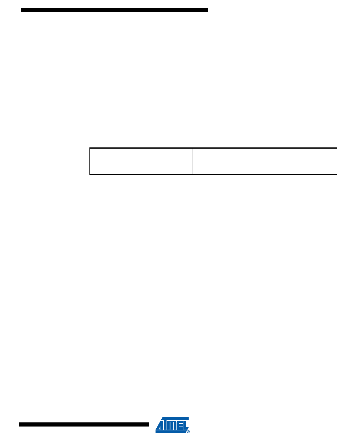
27.7.12 Programming Time for Flash when Using SPM
The calibrated RC Oscillator is used to time Flash accesses. Table 27-6 shows the typical pro-
gramming time for Flash accesses from the CPU.
27.7.13 Simple Assembly Code Example for a Boot Loader
;-the routine writes one page of data from RAM to Flash
; the first data location in RAM is pointed to by the Y pointer
; the first data location in Flash is pointed to by the Z-pointer
;-error handling is not included
;-the routine must be placed inside the Boot space
; (at least the Do_spm sub routine). Only code inside NRWW section can
; be read during Self-Programming (Page Erase and Page Write).
;-registers used: r0, r1, temp1 (r16), temp2 (r17), looplo (r24),
; loophi (r25), spmcrval (r20)
; storing and restoring of registers is not included in the routine
; register usage can be optimized at the expense of code size
;-It is assumed that either the interrupt table is moved to the Boot
; loader section or that the interrupts are disabled.
.equ PAGESIZEB = PAGESIZE*2 ;PAGESIZEB is page size in BYTES, not words
.org SMALLBOOTSTART
Write_page:
; Page Erase
ldi spmcrval, (1<<PGERS) | (1<<SPMEN)
call Do_spm
; re-enable the RWW section
ldi spmcrval, (1<<RWWSRE) | (1<<SPMEN)
call Do_spm
; transfer data from RAM to Flash page buffer
ldi looplo, low(PAGESIZEB) ;init loop variable
ldi loophi, high(PAGESIZEB) ;not required for PAGESIZEB<=256
Wrloop:
ld r0, Y+
ld r1, Y+
ldi spmcrval, (1<<SPMEN)
call Do_spm
adiw ZH:ZL, 2
sbiw loophi:looplo, 2 ;use subi for PAGESIZEB<=256
Table 27-6. SPM Programming Time
Symbol Min Programming Time Max Programming Time
Flash write (Page Erase, Page Write, and
write Lock bits by SPM)
3.7 ms 4.5 ms