
Manual


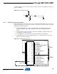


Table Of Contents
- Features
- 1. Pin Configurations
- 2. Overview
- 3. Disclaimer
- 4. Resources
- 5. About Code Examples
- 6. Data Retention
- 7. AVR CPU Core
- 8. Memories
- 9. System Clock and their Distribution
- 10. Power Management and Sleep Modes
- 11. System Control and Reset
- 12. Interrupts
- 13. External Interrupts
- 13.1 Pin Change Interrupt Timing
- 13.2 Register Description
- 13.2.1 EICRA – External Interrupt Control Register A
- 13.2.2 EIMSK – External Interrupt Mask Register
- 13.2.3 EIFR – External Interrupt Flag Register
- 13.2.4 PCICR – Pin Change Interrupt Control Register
- 13.2.5 PCIFR – Pin Change Interrupt Flag Register
- 13.2.6 PCMSK3 – Pin Change Mask Register 3
- 13.2.7 PCMSK2 – Pin Change Mask Register 2
- 13.2.8 PCMSK1 – Pin Change Mask Register 1
- 13.2.9 PCMSK0 – Pin Change Mask Register 0
- 14. I/O-Ports
- 14.1 Overview
- 14.2 Ports as General Digital I/O
- 14.3 Alternate Port Functions
- 14.4 Register Description
- 14.4.1 MCUCR – MCU Control Register
- 14.4.2 PORTB – Port B Data Register
- 14.4.3 DDRB – Port B Data Direction Register
- 14.4.4 PINB – Port B Input Pins Address
- 14.4.5 PORTC – Port C Data Register
- 14.4.6 DDRC – Port C Data Direction Register
- 14.4.7 PINC – Port C Input Pins Address
- 14.4.8 PORTD – Port D Data Register
- 14.4.9 DDRD – Port D Data Direction Register
- 14.4.10 PIND – Port D Input Pins Address
- 14.4.11 PORTE – Port E Data Register
- 14.4.12 DDRE – Port E Data Direction Register
- 14.4.13 PINE – Port E Input Pins Address
- 15. 8-bit Timer/Counter0 with PWM
- 15.1 Features
- 15.2 Overview
- 15.3 Timer/Counter Clock Sources
- 15.4 Counter Unit
- 15.5 Output Compare Unit
- 15.6 Compare Match Output Unit
- 15.7 Modes of Operation
- 15.8 Timer/Counter Timing Diagrams
- 15.9 Register Description
- 15.9.1 TCCR0A – Timer/Counter Control Register A
- 15.9.2 TCCR0B – Timer/Counter Control Register B
- 15.9.3 TCNT0 – Timer/Counter Register
- 15.9.4 OCR0A – Output Compare Register A
- 15.9.5 OCR0B – Output Compare Register B
- 15.9.6 TIMSK0 – Timer/Counter Interrupt Mask Register
- 15.9.7 TIFR0 – Timer/Counter 0 Interrupt Flag Register
- 16. 16-bit Timer/Counter1 with PWM
- 16.1 Features
- 16.2 Overview
- 16.3 Accessing 16-bit Registers
- 16.4 Timer/Counter Clock Sources
- 16.5 Counter Unit
- 16.6 Input Capture Unit
- 16.7 Output Compare Units
- 16.8 Compare Match Output Unit
- 16.9 Modes of Operation
- 16.10 Timer/Counter Timing Diagrams
- 16.11 Register Description
- 16.11.1 TCCR1A – Timer/Counter1 Control Register A
- 16.11.2 TCCR1B – Timer/Counter1 Control Register B
- 16.11.3 TCCR1C – Timer/Counter1 Control Register C
- 16.11.4 TCNT1H and TCNT1L – Timer/Counter1
- 16.11.5 OCR1AH and OCR1AL – Output Compare Register 1 A
- 16.11.6 OCR1BH and OCR1BL – Output Compare Register 1 B
- 16.11.7 ICR1H and ICR1L – Input Capture Register 1
- 16.11.8 TIMSK1 – Timer/Counter1 Interrupt Mask Register
- 16.11.9 TIFR1 – Timer/Counter1 Interrupt Flag Register
- 17. Timer/Counter0 and Timer/Counter1 Prescalers
- 18. PSC – Power Stage Controller
- 18.1 Features
- 18.2 Overview
- 18.3 Accessing 16-bit Registers
- 18.4 PSC Description
- 18.5 Functional Description
- 18.6 Update of Values
- 18.7 Overlap Protection
- 18.8 Signal Description
- 18.9 PSC Input
- 18.10 PSC Input Modes 001b to 10xb: Deactivate outputs without changing timing.
- 18.11 PSC Input Mode 11xb: Halt PSC and Wait for Software Action
- 18.12 Analog Synchronization
- 18.13 Interrupt Handling
- 18.14 PSC Clock Sources
- 18.15 Interrupts
- 18.16 Register Description
- 18.16.1 POC – PSC Output Configuration
- 18.16.2 PSYNC – PSC Synchro Configuration
- 18.16.3 POCRnSAH and POCRnSAL – PSC Output Compare SA Register
- 18.16.4 POCRnRAH and POCRnRAL – PSC Output Compare RA Register
- 18.16.5 POCRnSBH and POCRnSBL – PSCOutput Compare SB Register
- 18.16.6 POCRnRBH and POCRnRBL – PSC Output Compare RB Register
- 18.16.7 PCNF – PSC Configuration Register
- 18.16.8 PCTL – PSC Control Register
- 18.16.9 PMICn – PSC Module n Input Control Register
- 18.16.10 PSC Interrupt Mask Register – PIM
- 18.16.11 PIFR – PSC Interrupt Flag Register
- 19. SPI – Serial Peripheral Interface
- 20. CAN – Controller Area Network
- 20.1 Features
- 20.2 Overview
- 20.3 CAN Protocol
- 20.3.1 Principles
- 20.3.2 Message Formats
- 20.3.3 CAN Bit Timing
- 20.3.3.1 Bit Construction
- 20.3.3.2 Synchronization Segment
- 20.3.3.3 Propagation Time Segment
- 20.3.3.4 Phase Segment 1
- 20.3.3.5 Sample Point
- 20.3.3.6 Phase Segment 2
- 20.3.3.7 Information Processing Time
- 20.3.3.8 Bit Lengthening
- 20.3.3.9 Bit Shortening
- 20.3.3.10 Synchronization Jump Width
- 20.3.3.11 Programming the Sample Point
- 20.3.3.12 Synchronization
- 20.3.4 Arbitration
- 20.3.5 Errors
- 20.4 CAN Controller
- 20.5 CAN Channel
- 20.6 Message Objects
- 20.7 CAN Timer
- 20.8 Error Management
- 20.9 Interrupts
- 20.10 Register Description
- 20.10.1 CANGCON – CAN General Control Register
- 20.10.2 CANGSTA – CAN General Status Register
- 20.10.3 CANGIT – CAN General Interrupt Register
- 20.10.4 CANGIE – CAN General Interrupt Enable Register
- 20.10.5 CANEN2 and CANEN1 – CAN Enable MOb Registers
- 20.10.6 CANIE2 and CANIE1 – CAN Enable Interrupt MOb Registers
- 20.10.7 CANSIT2 and CANSIT1 – CAN Status Interrupt MOb Registers
- 20.10.8 CANBT1 – CAN Bit Timing Register 1
- 20.10.9 CANBT2 – CAN Bit Timing Register 2
- 20.10.10 CANBT3 – CAN Bit Timing Register 3
- 20.10.11 CANTCON – CAN Timer Control Register
- 20.10.12 CANTIML and CANTIMH – CAN Timer Registers
- 20.10.13 CANTTCL and CANTTCH – CAN TTC Timer Registers
- 20.10.14 CANTEC – CAN Transmit Error Counter Register
- 20.10.15 CANREC – CAN Receive Error Counter Register
- 20.10.16 CANHPMOB – CAN Highest Priority MOb Register
- 20.10.17 CANPAGE – CAN Page MOb Register
- 20.11 MOb Registers
- 20.11.1 CANSTMOB – CAN MOb Status Register
- 20.11.2 CANCDMOB – CAN MOb Control and DLC Register
- 20.11.3 CANIDT1, CANIDT2, CANIDT3, and CANIDT4 – CAN Identifier Tag Registers
- 20.11.4 CANIDM1, CANIDM2, CANIDM3, and CANIDM4 – CAN Identifier Mask Registers
- 20.11.5 CANSTML and CANSTMH – CAN Time Stamp Registers
- 20.11.6 CANMSG – CAN Data Message Register
- 20.12 Examples of CAN Baud Rate Setting
- 21. LIN / UART - Local Interconnect Network Controller or UART
- 21.1 Features
- 21.2 Overview
- 21.3 LIN Protocol
- 21.4 LIN / UART Controller
- 21.5 LIN / UART Description
- 21.5.1 Reset
- 21.5.2 Clock
- 21.5.3 LIN Protocol Selection
- 21.5.4 Configuration
- 21.5.5 Busy Signal
- 21.5.6 Bit Timing
- 21.5.7 Data Length
- 21.5.8 xxOK Flags
- 21.5.9 xxERR Flags
- 21.5.10 Frame Time Out
- 21.5.11 Break-in-data
- 21.5.12 Checksum
- 21.5.13 Interrupts
- 21.5.14 Message Filtering
- 21.5.15 Data Management
- 21.5.16 OCD Support
- 21.6 Register Description
- 21.6.1 LINCR – LIN Control Register
- 21.6.2 LINSIR – LIN Status and Interrupt Register
- 21.6.3 LINENIR – LIN Enable Interrupt Register
- 21.6.4 LINERR – LIN Error Register
- 21.6.5 LINBTR – LIN Bit Timing Register
- 21.6.6 LINBRR – LIN Baud Rate Register
- 21.6.7 LINDLR – LIN Data Length Register
- 21.6.8 LINIDR – LIN Identifier Register
- 21.6.9 LINSEL – LIN Data Buffer Selection Register
- 21.6.10 LINDAT – LIN Data Register
- 22. ADC – Analog to Digital Converter
- 22.1 Features
- 22.2 Operation
- 22.3 Starting a Conversion
- 22.4 Prescaling and Conversion Timing
- 22.5 Changing Channel or Reference Selection
- 22.6 ADC Noise Canceler
- 22.7 ADC Conversion Result
- 22.8 Temperature Measurement
- 22.9 Amplifier
- 22.10 Register Description
- 22.10.1 ADMUX – ADC Multiplexer Register
- 22.10.2 Bit 4: 0 – MUX[4:0]: ADC Channel Selection Bits
- 22.10.3 ADCSRA – ADC Control and Status Register A
- 22.10.4 ADCSRB – ADC Control and Status Register B
- 22.10.5 ADCH and ADCL – ADC Result Data Registers
- 22.10.6 DIDR0 – Digital Input Disable Register 0
- 22.10.7 DIDR1 – Digital Input Disable Register 1
- 22.10.8 AMP0CSR – Amplifier 0 Control and Status register
- 22.10.9 AMP1CSR – Amplifier 1 Control and Status register
- 22.10.10 AMP2CSR – Amplifier 2 Control and Status register
- 23. ISRC - Current Source
- 24. AC – Analog Comparator
- 24.1 Features
- 24.2 Overview
- 24.3 Use of ADC Amplifiers
- 24.4 Register Description
- 24.4.1 AC0CON – Analog Comparator 0 Control Register
- 24.4.2 AC1CON – Analog Comparator 1Control Register
- 24.4.3 AC2CON – Analog Comparator 2 Control Register
- 24.4.4 AC3CON – Analog Comparator 3 Control Register
- 24.4.5 ACSR – Analog Comparator Status Register
- 24.4.6 DIDR0 – Digital Input Disable Register 0
- 24.4.7 DIDR1 – Digital Input Disable Register 1
- 25. DAC – Digital to Analog Converter
- 26. debugWIRE On-chip Debug System
- 27. Boot Loader Support – Read-While-Write Self-Programming
- 27.1 Overview
- 27.2 Application and Boot Loader Flash Sections
- 27.3 Read-While-Write and No Read-While-Write Flash Sections
- 27.4 Boot Loader Lock Bits
- 27.5 Entering the Boot Loader Program
- 27.6 Addressing the Flash During Self-Programming
- 27.7 Self-Programming the Flash
- 27.7.1 Performing Page Erase by SPM
- 27.7.2 Filling the Temporary Buffer (Page Loading)
- 27.7.3 Performing a Page Write
- 27.7.4 Using the SPM Interrupt
- 27.7.5 Consideration While Updating BLS
- 27.7.6 Prevent Reading the RWW Section During Self-Programming
- 27.7.7 Setting the Boot Loader Lock Bits by SPM
- 27.7.8 EEPROM Write Prevents Writing to SPMCSR
- 27.7.9 Reading the Fuse and Lock Bits from Software
- 27.7.10 Reading the Signature Row from Software
- 27.7.11 Preventing Flash Corruption
- 27.7.12 Programming Time for Flash when Using SPM
- 27.7.13 Simple Assembly Code Example for a Boot Loader
- 27.7.14 ATmega16M1 - 16K - Flash Boot Loader Parameters
- 27.7.15 ATmega32M1 - 32K - Flash Boot Loader Parameters
- 27.7.16 ATmega64M1 - 64K - Flash Boot Loader Parameters
- 27.8 Register Description
- 28. Memory Programming
- 28.1 Program And Data Memory Lock Bits
- 28.2 Fuse Bits
- 28.3 PSC Output Behavior During Reset
- 28.4 Signature Bytes
- 28.5 Calibration Byte
- 28.6 Page Size
- 28.7 Parallel Programming Parameters, Pin Mapping, and Commands
- 28.8 Serial Programming Pin Mapping
- 28.9 Parallel Programming
- 28.9.1 Enter Programming Mode
- 28.9.2 Considerations for Efficient Programming
- 28.9.3 Chip Erase
- 28.9.4 Programming the Flash
- 28.9.5 Programming the EEPROM
- 28.9.6 Reading the Flash
- 28.9.7 Reading the EEPROM
- 28.9.8 Programming the Fuse Low Bits
- 28.9.9 Programming the Fuse High Bits
- 28.9.10 Programming the Extended Fuse Bits
- 28.9.11 Programming the Lock Bits
- 28.9.12 Reading the Fuse and Lock Bits
- 28.9.13 Reading the Signature Bytes
- 28.9.14 Reading the Calibration Byte
- 28.9.15 Parallel Programming Characteristics
- 28.10 Serial Downloading
- 29. Electrical Characteristics
- 30. Typical Characteristics – TBD
- 31. Register Summary
- 32. Instruction Set Summary
- 33. Errata
- 34. Ordering Information
- 35. Packaging Information
- 36. Datasheet Revision History
- Table of Contents

239
8209A–AVR–08/09
ATmega16M1/32M1/64M1
The measured voltage has a linear relationship to the temperature as described in Table 22-3 on
page 239. The voltage sensitivity is approximately 1 mV/
°C and the accuracy of the temperature
measurement is +/- 10°C after bandgap calibration.
The values described in Table 22-3 on page 239 are typical values. However, due to the process
variation the temperature sensor output voltage varies from one chip to another. To be capable
of achieving more accurate results, the temperature measurement can be calibrated in the appli-
cation software.
22.8.1 User Calibration
The software calibration requires that a calibration value is measured and stored in a register or
EEPROM for each chip. The software calibration can be done utilizing the formula:
T = { [ (ADCH << 8) | ADCL ] - T
OS
} / k
where ADCH & ADCL are the ADC data registers, k is a fixed coefficient and T
OS
is the temper-
ature sensor offset value determined and stored into EEPROM.
22.8.2 Manufacturing Calibration
One can also use the calibration values available in the signature row See “Reading the Signa-
ture Row from Software” on page 281.
The calibration values are determined from values measured during test at room temperature
which is approximatively +25°C and during test at hot temperature which is approximatively
+85°C.
The temperature in Celsius degrees can be calculated utilizing the formula:
T = { [ (ADCH << 8) | ADCL ] *TSGAIN } +TSOFFSET-273
Where:
a. ADCH & ADCL are the ADC data registers,
b. TSGAIN is the temperature sensor gain (constant 1, or unsigned fixed point num-
ber, 0x80 = decimal 1.0)
c. TSOFFSET is the temperature sensor offset correction term (2. complement
signed byte)
22.9 Amplifier
The ATmega16M1/32M1/64M1 features three differential amplified channels with programmable
5, 10, 20, and 40 gain stage.
Because the amplifiers are switching capacitor amplifiers, they need to be clocked by a synchro-
nization signal called in this document the amplifier synchronization clock. To ensure an
accurate result, the amplifier input needs to have a quite stable input value during at least 4
Amplifier synchronization clock periods.
To ensure an accurate result, the amplifier input needs to have a quite stable input value at the
sampling point during at least 4 amplifier synchronization clock periods.
Table 22-3. Temperature vs. Sensor Output Voltage (Typical Case)
Temperature / °C-40 °C+25 °C +85 °C
Voltage / mV 600 mV 762 mv TBD mV