
Manual


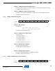


Table Of Contents
- Features
- 1. Pin Configurations
- 2. Overview
- 3. Disclaimer
- 4. Resources
- 5. About Code Examples
- 6. Data Retention
- 7. AVR CPU Core
- 8. Memories
- 9. System Clock and their Distribution
- 10. Power Management and Sleep Modes
- 11. System Control and Reset
- 12. Interrupts
- 13. External Interrupts
- 13.1 Pin Change Interrupt Timing
- 13.2 Register Description
- 13.2.1 EICRA – External Interrupt Control Register A
- 13.2.2 EIMSK – External Interrupt Mask Register
- 13.2.3 EIFR – External Interrupt Flag Register
- 13.2.4 PCICR – Pin Change Interrupt Control Register
- 13.2.5 PCIFR – Pin Change Interrupt Flag Register
- 13.2.6 PCMSK3 – Pin Change Mask Register 3
- 13.2.7 PCMSK2 – Pin Change Mask Register 2
- 13.2.8 PCMSK1 – Pin Change Mask Register 1
- 13.2.9 PCMSK0 – Pin Change Mask Register 0
- 14. I/O-Ports
- 14.1 Overview
- 14.2 Ports as General Digital I/O
- 14.3 Alternate Port Functions
- 14.4 Register Description
- 14.4.1 MCUCR – MCU Control Register
- 14.4.2 PORTB – Port B Data Register
- 14.4.3 DDRB – Port B Data Direction Register
- 14.4.4 PINB – Port B Input Pins Address
- 14.4.5 PORTC – Port C Data Register
- 14.4.6 DDRC – Port C Data Direction Register
- 14.4.7 PINC – Port C Input Pins Address
- 14.4.8 PORTD – Port D Data Register
- 14.4.9 DDRD – Port D Data Direction Register
- 14.4.10 PIND – Port D Input Pins Address
- 14.4.11 PORTE – Port E Data Register
- 14.4.12 DDRE – Port E Data Direction Register
- 14.4.13 PINE – Port E Input Pins Address
- 15. 8-bit Timer/Counter0 with PWM
- 15.1 Features
- 15.2 Overview
- 15.3 Timer/Counter Clock Sources
- 15.4 Counter Unit
- 15.5 Output Compare Unit
- 15.6 Compare Match Output Unit
- 15.7 Modes of Operation
- 15.8 Timer/Counter Timing Diagrams
- 15.9 Register Description
- 15.9.1 TCCR0A – Timer/Counter Control Register A
- 15.9.2 TCCR0B – Timer/Counter Control Register B
- 15.9.3 TCNT0 – Timer/Counter Register
- 15.9.4 OCR0A – Output Compare Register A
- 15.9.5 OCR0B – Output Compare Register B
- 15.9.6 TIMSK0 – Timer/Counter Interrupt Mask Register
- 15.9.7 TIFR0 – Timer/Counter 0 Interrupt Flag Register
- 16. 16-bit Timer/Counter1 with PWM
- 16.1 Features
- 16.2 Overview
- 16.3 Accessing 16-bit Registers
- 16.4 Timer/Counter Clock Sources
- 16.5 Counter Unit
- 16.6 Input Capture Unit
- 16.7 Output Compare Units
- 16.8 Compare Match Output Unit
- 16.9 Modes of Operation
- 16.10 Timer/Counter Timing Diagrams
- 16.11 Register Description
- 16.11.1 TCCR1A – Timer/Counter1 Control Register A
- 16.11.2 TCCR1B – Timer/Counter1 Control Register B
- 16.11.3 TCCR1C – Timer/Counter1 Control Register C
- 16.11.4 TCNT1H and TCNT1L – Timer/Counter1
- 16.11.5 OCR1AH and OCR1AL – Output Compare Register 1 A
- 16.11.6 OCR1BH and OCR1BL – Output Compare Register 1 B
- 16.11.7 ICR1H and ICR1L – Input Capture Register 1
- 16.11.8 TIMSK1 – Timer/Counter1 Interrupt Mask Register
- 16.11.9 TIFR1 – Timer/Counter1 Interrupt Flag Register
- 17. Timer/Counter0 and Timer/Counter1 Prescalers
- 18. PSC – Power Stage Controller
- 18.1 Features
- 18.2 Overview
- 18.3 Accessing 16-bit Registers
- 18.4 PSC Description
- 18.5 Functional Description
- 18.6 Update of Values
- 18.7 Overlap Protection
- 18.8 Signal Description
- 18.9 PSC Input
- 18.10 PSC Input Modes 001b to 10xb: Deactivate outputs without changing timing.
- 18.11 PSC Input Mode 11xb: Halt PSC and Wait for Software Action
- 18.12 Analog Synchronization
- 18.13 Interrupt Handling
- 18.14 PSC Clock Sources
- 18.15 Interrupts
- 18.16 Register Description
- 18.16.1 POC – PSC Output Configuration
- 18.16.2 PSYNC – PSC Synchro Configuration
- 18.16.3 POCRnSAH and POCRnSAL – PSC Output Compare SA Register
- 18.16.4 POCRnRAH and POCRnRAL – PSC Output Compare RA Register
- 18.16.5 POCRnSBH and POCRnSBL – PSCOutput Compare SB Register
- 18.16.6 POCRnRBH and POCRnRBL – PSC Output Compare RB Register
- 18.16.7 PCNF – PSC Configuration Register
- 18.16.8 PCTL – PSC Control Register
- 18.16.9 PMICn – PSC Module n Input Control Register
- 18.16.10 PSC Interrupt Mask Register – PIM
- 18.16.11 PIFR – PSC Interrupt Flag Register
- 19. SPI – Serial Peripheral Interface
- 20. CAN – Controller Area Network
- 20.1 Features
- 20.2 Overview
- 20.3 CAN Protocol
- 20.3.1 Principles
- 20.3.2 Message Formats
- 20.3.3 CAN Bit Timing
- 20.3.3.1 Bit Construction
- 20.3.3.2 Synchronization Segment
- 20.3.3.3 Propagation Time Segment
- 20.3.3.4 Phase Segment 1
- 20.3.3.5 Sample Point
- 20.3.3.6 Phase Segment 2
- 20.3.3.7 Information Processing Time
- 20.3.3.8 Bit Lengthening
- 20.3.3.9 Bit Shortening
- 20.3.3.10 Synchronization Jump Width
- 20.3.3.11 Programming the Sample Point
- 20.3.3.12 Synchronization
- 20.3.4 Arbitration
- 20.3.5 Errors
- 20.4 CAN Controller
- 20.5 CAN Channel
- 20.6 Message Objects
- 20.7 CAN Timer
- 20.8 Error Management
- 20.9 Interrupts
- 20.10 Register Description
- 20.10.1 CANGCON – CAN General Control Register
- 20.10.2 CANGSTA – CAN General Status Register
- 20.10.3 CANGIT – CAN General Interrupt Register
- 20.10.4 CANGIE – CAN General Interrupt Enable Register
- 20.10.5 CANEN2 and CANEN1 – CAN Enable MOb Registers
- 20.10.6 CANIE2 and CANIE1 – CAN Enable Interrupt MOb Registers
- 20.10.7 CANSIT2 and CANSIT1 – CAN Status Interrupt MOb Registers
- 20.10.8 CANBT1 – CAN Bit Timing Register 1
- 20.10.9 CANBT2 – CAN Bit Timing Register 2
- 20.10.10 CANBT3 – CAN Bit Timing Register 3
- 20.10.11 CANTCON – CAN Timer Control Register
- 20.10.12 CANTIML and CANTIMH – CAN Timer Registers
- 20.10.13 CANTTCL and CANTTCH – CAN TTC Timer Registers
- 20.10.14 CANTEC – CAN Transmit Error Counter Register
- 20.10.15 CANREC – CAN Receive Error Counter Register
- 20.10.16 CANHPMOB – CAN Highest Priority MOb Register
- 20.10.17 CANPAGE – CAN Page MOb Register
- 20.11 MOb Registers
- 20.11.1 CANSTMOB – CAN MOb Status Register
- 20.11.2 CANCDMOB – CAN MOb Control and DLC Register
- 20.11.3 CANIDT1, CANIDT2, CANIDT3, and CANIDT4 – CAN Identifier Tag Registers
- 20.11.4 CANIDM1, CANIDM2, CANIDM3, and CANIDM4 – CAN Identifier Mask Registers
- 20.11.5 CANSTML and CANSTMH – CAN Time Stamp Registers
- 20.11.6 CANMSG – CAN Data Message Register
- 20.12 Examples of CAN Baud Rate Setting
- 21. LIN / UART - Local Interconnect Network Controller or UART
- 21.1 Features
- 21.2 Overview
- 21.3 LIN Protocol
- 21.4 LIN / UART Controller
- 21.5 LIN / UART Description
- 21.5.1 Reset
- 21.5.2 Clock
- 21.5.3 LIN Protocol Selection
- 21.5.4 Configuration
- 21.5.5 Busy Signal
- 21.5.6 Bit Timing
- 21.5.7 Data Length
- 21.5.8 xxOK Flags
- 21.5.9 xxERR Flags
- 21.5.10 Frame Time Out
- 21.5.11 Break-in-data
- 21.5.12 Checksum
- 21.5.13 Interrupts
- 21.5.14 Message Filtering
- 21.5.15 Data Management
- 21.5.16 OCD Support
- 21.6 Register Description
- 21.6.1 LINCR – LIN Control Register
- 21.6.2 LINSIR – LIN Status and Interrupt Register
- 21.6.3 LINENIR – LIN Enable Interrupt Register
- 21.6.4 LINERR – LIN Error Register
- 21.6.5 LINBTR – LIN Bit Timing Register
- 21.6.6 LINBRR – LIN Baud Rate Register
- 21.6.7 LINDLR – LIN Data Length Register
- 21.6.8 LINIDR – LIN Identifier Register
- 21.6.9 LINSEL – LIN Data Buffer Selection Register
- 21.6.10 LINDAT – LIN Data Register
- 22. ADC – Analog to Digital Converter
- 22.1 Features
- 22.2 Operation
- 22.3 Starting a Conversion
- 22.4 Prescaling and Conversion Timing
- 22.5 Changing Channel or Reference Selection
- 22.6 ADC Noise Canceler
- 22.7 ADC Conversion Result
- 22.8 Temperature Measurement
- 22.9 Amplifier
- 22.10 Register Description
- 22.10.1 ADMUX – ADC Multiplexer Register
- 22.10.2 Bit 4: 0 – MUX[4:0]: ADC Channel Selection Bits
- 22.10.3 ADCSRA – ADC Control and Status Register A
- 22.10.4 ADCSRB – ADC Control and Status Register B
- 22.10.5 ADCH and ADCL – ADC Result Data Registers
- 22.10.6 DIDR0 – Digital Input Disable Register 0
- 22.10.7 DIDR1 – Digital Input Disable Register 1
- 22.10.8 AMP0CSR – Amplifier 0 Control and Status register
- 22.10.9 AMP1CSR – Amplifier 1 Control and Status register
- 22.10.10 AMP2CSR – Amplifier 2 Control and Status register
- 23. ISRC - Current Source
- 24. AC – Analog Comparator
- 24.1 Features
- 24.2 Overview
- 24.3 Use of ADC Amplifiers
- 24.4 Register Description
- 24.4.1 AC0CON – Analog Comparator 0 Control Register
- 24.4.2 AC1CON – Analog Comparator 1Control Register
- 24.4.3 AC2CON – Analog Comparator 2 Control Register
- 24.4.4 AC3CON – Analog Comparator 3 Control Register
- 24.4.5 ACSR – Analog Comparator Status Register
- 24.4.6 DIDR0 – Digital Input Disable Register 0
- 24.4.7 DIDR1 – Digital Input Disable Register 1
- 25. DAC – Digital to Analog Converter
- 26. debugWIRE On-chip Debug System
- 27. Boot Loader Support – Read-While-Write Self-Programming
- 27.1 Overview
- 27.2 Application and Boot Loader Flash Sections
- 27.3 Read-While-Write and No Read-While-Write Flash Sections
- 27.4 Boot Loader Lock Bits
- 27.5 Entering the Boot Loader Program
- 27.6 Addressing the Flash During Self-Programming
- 27.7 Self-Programming the Flash
- 27.7.1 Performing Page Erase by SPM
- 27.7.2 Filling the Temporary Buffer (Page Loading)
- 27.7.3 Performing a Page Write
- 27.7.4 Using the SPM Interrupt
- 27.7.5 Consideration While Updating BLS
- 27.7.6 Prevent Reading the RWW Section During Self-Programming
- 27.7.7 Setting the Boot Loader Lock Bits by SPM
- 27.7.8 EEPROM Write Prevents Writing to SPMCSR
- 27.7.9 Reading the Fuse and Lock Bits from Software
- 27.7.10 Reading the Signature Row from Software
- 27.7.11 Preventing Flash Corruption
- 27.7.12 Programming Time for Flash when Using SPM
- 27.7.13 Simple Assembly Code Example for a Boot Loader
- 27.7.14 ATmega16M1 - 16K - Flash Boot Loader Parameters
- 27.7.15 ATmega32M1 - 32K - Flash Boot Loader Parameters
- 27.7.16 ATmega64M1 - 64K - Flash Boot Loader Parameters
- 27.8 Register Description
- 28. Memory Programming
- 28.1 Program And Data Memory Lock Bits
- 28.2 Fuse Bits
- 28.3 PSC Output Behavior During Reset
- 28.4 Signature Bytes
- 28.5 Calibration Byte
- 28.6 Page Size
- 28.7 Parallel Programming Parameters, Pin Mapping, and Commands
- 28.8 Serial Programming Pin Mapping
- 28.9 Parallel Programming
- 28.9.1 Enter Programming Mode
- 28.9.2 Considerations for Efficient Programming
- 28.9.3 Chip Erase
- 28.9.4 Programming the Flash
- 28.9.5 Programming the EEPROM
- 28.9.6 Reading the Flash
- 28.9.7 Reading the EEPROM
- 28.9.8 Programming the Fuse Low Bits
- 28.9.9 Programming the Fuse High Bits
- 28.9.10 Programming the Extended Fuse Bits
- 28.9.11 Programming the Lock Bits
- 28.9.12 Reading the Fuse and Lock Bits
- 28.9.13 Reading the Signature Bytes
- 28.9.14 Reading the Calibration Byte
- 28.9.15 Parallel Programming Characteristics
- 28.10 Serial Downloading
- 29. Electrical Characteristics
- 30. Typical Characteristics – TBD
- 31. Register Summary
- 32. Instruction Set Summary
- 33. Errata
- 34. Ordering Information
- 35. Packaging Information
- 36. Datasheet Revision History
- Table of Contents
228
8209A–AVR–08/09
ATmega16M1/32M1/64M1
Figure 22-2. ADC Auto Trigger Logic
Using the ADC Interrupt Flag as a trigger source makes the ADC start a new conversion as soon
as the ongoing conversion has finished. The ADC then operates in Free Running mode, con-
stantly sampling and updating the ADC Data Register. The first conversion must be started by
writing a logical one to the ADSC bit in ADCSRA. In this mode the ADC will perform successive
conversions independently of whether the ADC Interrupt Flag, ADIF is cleared or not. The free
running mode is not allowed on the amplified channels.
If Auto Triggering is enabled, single conversions can be started by writing ADSC in ADCSRA to
one. ADSC can also be used to determine if a conversion is in progress. The ADSC bit will be
read as one during a conversion, independently of how the conversion was started.
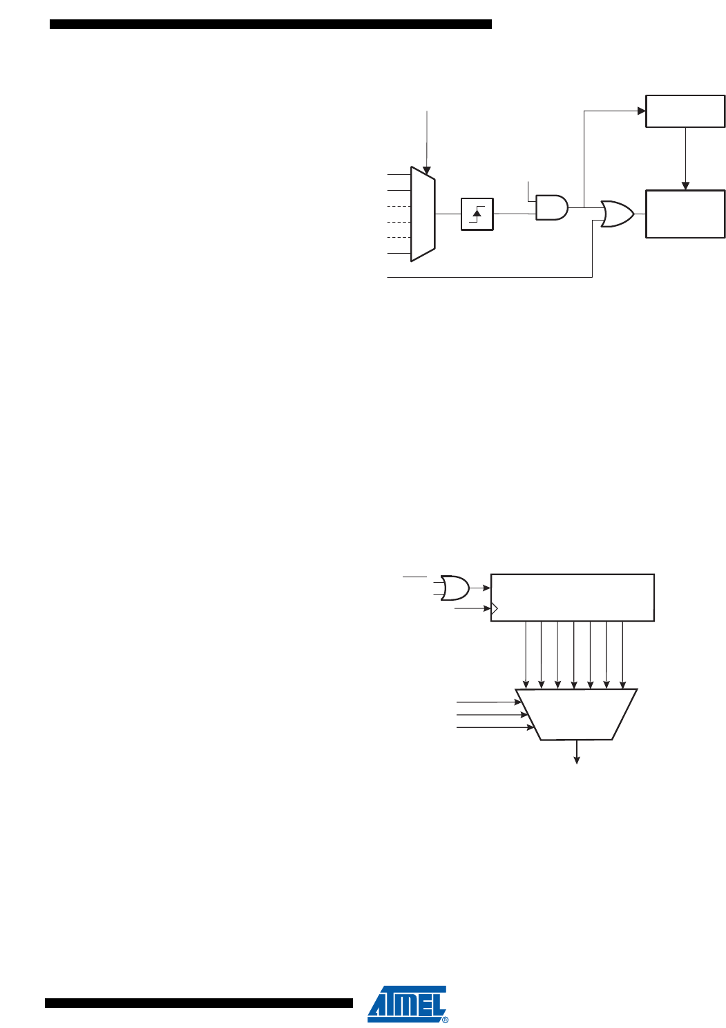
22.4 Prescaling and Conversion Timing
Figure 22-3. ADC Prescaler
By default, the successive approximation circuitry requires an input clock frequency between 50
kHz and 2 MHz to get maximum resolution. If a lower resolution than 10 bits is needed, the input
clock frequency to the ADC can be higher than 2 MHz to get a higher sample rate.
The ADC module contains a prescaler, which generates an acceptable ADC clock frequency
from any CPU frequency above 100 kHz. The prescaling is set by the ADPS bits in ADCSRA.
The prescaler starts counting from the moment the ADC is switched on by setting the ADEN bit
in ADCSRA. The prescaler keeps running for as long as the ADEN bit is set, and is continuously
reset when ADEN is low.
ADSC
ADIF
SOURCE 1
SOURCE n
ADTS[2:0]
CONVERSION
LOGIC
PRESCALER
START
CLK
ADC
.
.
.
.
EDGE
DETECTOR
ADATE
7-BIT ADC PRESCALER
ADC CLOCK SOURCE
CK
ADPS0
ADPS1
ADPS2
CK/128
CK/2
CK/4
CK/8
CK/16
CK/32
CK/64
Reset
ADEN
START