Features • High-performance, Low-power AVR® 8-bit Microcontroller • Advanced RISC Architecture • • • • • • • – 131 Powerful Instructions – Most Single-clock Cycle Execution – 32 x 8 General Purpose Working Registers – Fully Static Operation – Up to 16 MIPS Throughput at 16 MHz – On-chip 2-cycle Multiplier Nonvolatile Program and Data Memories – 32K Bytes of In-System Self-Programmable Flash Endurance: 10,000 Write/Erase Cycles – Optional Boot Code Section with Independent Lock Bits In-System Programmi
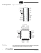
Pin Configurations Figure 1.
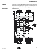
ATmega32(L) Overview The ATmega32 is a low-power CMOS 8-bit microcontroller based on the AVR enhanced RISC architecture. By executing powerful instructions in a single clock cycle, the ATmega32 achieves throughputs approaching 1 MIPS per MHz allowing the system designer to optimize power consumption versus processing speed. Block Diagram Figure 2.
The AVR core combines a rich instruction set with 32 general purpose working registers. All the 32 registers are directly connected to the Arithmetic Logic Unit (ALU), allowing two independent registers to be accessed in one single instruction executed in one clock cycle. The resulting architecture is more code efficient while achieving throughputs up to ten times faster than conventional CISC microcontrollers.
ATmega32(L) Port B (PB7..PB0) Port B is an 8-bit bi-directional I/O port with internal pull-up resistors (selected for each bit). The Port B output buffers have symmetrical drive characteristics with both high sink and source capability. As inputs, Port B pins that are externally pulled low will source current if the pull-up resistors are activated. The Port B pins are tri-stated when a reset condition becomes active, even if the clock is not running.
AVR CPU Core Introduction This section discusses the AVR core architecture in general. The main function of the CPU core is to ensure correct program execution. The CPU must therefore be able to access memories, perform calculations, control peripherals, and handle interrupts. Architectural Overview Figure 3.
ATmega32(L) an arithmetic operation, the Status Register is updated to reflect information about the result of the operation. Program flow is provided by conditional and unconditional jump and call instructions, able to directly address the whole address space. Most AVR instructions have a single 16-bit word format. Every program memory address contains a 16- or 32-bit instruction. Program Flash memory space is divided in two sections, the Boot program section and the Application Program section.
Status Register The Status Register contains information about the result of the most recently executed arithmetic instruction. This information can be used for altering program flow in order to perform conditional operations. Note that the Status Register is updated after all ALU operations, as specified in the Instruction Set Reference. This will in many cases remove the need for using the dedicated compare instructions, resulting in faster and more compact code.
ATmega32(L) • Bit 0 – C: Carry Flag The Carry Flag C indicates a carry in an arithmetic or logic operation. See the “Instruction Set Description” for detailed information. General Purpose Register File The Register File is optimized for the AVR Enhanced RISC instruction set.
The X-register, Y-register and Z-register The registers R26..R31 have some added functions to their general purpose usage. These registers are 16-bit address pointers for indirect addressing of the Data Space. The three indirect address registers X, Y, and Z are defined as described in Figure 5. Figure 5.
ATmega32(L) Instruction Execution Timing This section describes the general access timing concepts for instruction execution. The AVR CPU is driven by the CPU clock clkCPU, directly generated from the selected clock source for the chip. No internal clock division is used. Figure 6 shows the parallel instruction fetches and instruction executions enabled by the Harvard architecture and the fast-access Register file concept.
– the External Interrupt Request 0. The Interrupt Vectors can be moved to the start of the Boot Flash section by setting the IVSEL bit in the General Interrupt Control Register (GICR). Refer to “Interrupts” on page 42 for more information. The Reset Vector can also be moved to the start of the boot Flash section by programming the BOOTRST fuse, see “Boot Loader Support – Read-While-Write Self-Programming” on page 242.
ATmega32(L) When using the SEI instruction to enable interrupts, the instruction following SEI will be executed before any pending interrupts, as shown in this example.
AVR ATmega32 Memories This section describes the different memories in the ATmega32. The AVR architecture has two main memory spaces, the Data Memory and the Program Memory space. In addition, the ATmega32 features an EEPROM Memory for data storage. All three memory spaces are linear and regular. In-System Reprogrammable Flash Program Memory The ATmega32 contains 32K bytes On-chip In-System Reprogrammable Flash memory for program storage.
ATmega32(L) SRAM Data Memory Figure 9 shows how the ATmega32 SRAM Memory is organized. The lower 2144 Data Memory locations address the Register file, the I/O Memory, and the internal data SRAM. The first 96 locations address the Register file and I/O Memory, and the next 2048 locations address the internal data SRAM. The five different addressing modes for the data memory cover: Direct, Indirect with Displacement, Indirect, Indirect with Pre-decrement, and Indirect with Post-increment.
Data Memory Access Times This section describes the general access timing concepts for internal memory access. The internal data SRAM access is performed in two clkCPU cycles as described in Figure 10. Figure 10. On-chip Data SRAM Access Cycles T1 T2 T3 clkCPU Address Compute Address Address Valid Write Data WR Read Data RD Memory Access Instruction EEPROM Data Memory Next Instruction The ATmega32 contains 1024 bytes of data EEPROM memory.
ATmega32(L) The EEPROM Address Register – EEARH and EEARL Bit Read/Write Initial Value 15 14 13 12 11 10 9 8 – – – – – – EEAR9 EEAR8 EEARH EEAR7 EEAR6 EEAR5 EEAR4 EEAR3 EEAR2 EEAR1 EEAR0 EEARL 7 6 5 4 3 2 1 0 R R R R R R R/W R/W R/W R/W R/W R/W R/W R/W R/W R/W 0 0 0 0 0 0 0 X X X X X X X X X • Bits 15..10 – Res: Reserved Bits These bits are reserved bits in the ATmega32 and will always read as zero. • Bits 9..0 – EEAR9..
When EEMWE has been written to one by software, hardware clears the bit to zero after four clock cycles. See the description of the EEWE bit for an EEPROM write procedure. • Bit 1 – EEWE: EEPROM Write Enable The EEPROM Write Enable Signal EEWE is the write strobe to the EEPROM. When address and data are correctly set up, the EEWE bit must be written to one to write the value into the EEPROM. The EEMWE bit must be written to one before a logical one is written to EEWE, otherwise no EEPROM write takes place.
ATmega32(L) The following code examples show one assembly and one C function for writing to the EEPROM. The examples assume that interrupts are controlled (for example by disabling interrupts globally) so that no interrupts will occur during execution of these functions. The examples also assume that no Flash Boot Loader is present in the software. If such code is present, the EEPROM write function must also wait for any ongoing SPM command to finish.
The next code examples show assembly and C functions for reading the EEPROM. The examples assume that interrupts are controlled so that no interrupts will occur during execution of these functions.
ATmega32(L) I/O Memory The I/O space definition of the ATmega32 is shown in “Register Summary” on page 297. All ATmega32 I/Os and peripherals are placed in the I/O space. The I/O locations are accessed by the IN and OUT instructions, transferring data between the 32 general purpose working registers and the I/O space. I/O Registers within the address range $00 $1F are directly bit-accessible using the SBI and CBI instructions.
System Clock and Clock Options Clock Systems and their Distribution Figure 11 presents the principal clock systems in the AVR and their distribution. All of the clocks need not be active at a given time. In order to reduce power consumption, the clocks to modules not being used can be halted by using different sleep modes, as described in “Power Management and Sleep Modes” on page 30. The clock systems are detailed Figure 11. Figure 11.
ATmega32(L) Asynchronous Timer Clock – clkASY The Asynchronous Timer clock allows the Asynchronous Timer/Counter to be clocked directly from an external 32 kHz clock crystal. The dedicated clock domain allows using this Timer/Counter as a real-time counter even when the device is in sleep mode. ADC Clock – clkADC The ADC is provided with a dedicated clock domain. This allows halting the CPU and I/O clocks in order to reduce noise generated by digital circuitry.
Crystal Oscillator XTAL1 and XTAL2 are input and output, respectively, of an inverting amplifier which can be configured for use as an On-chip Oscillator, as shown in Figure 12. Either a quartz crystal or a ceramic resonator may be used. The CKOPT Fuse selects between two different Oscillator amplifier modes. When CKOPT is programmed, the Oscillator output will oscillate will a full rail-to-rail swing on the output.
ATmega32(L) The CKSEL0 Fuse together with the SUT1..0 fuses select the start-up times as shown in Table 5. Table 5. Start-up Times for the Crystal Oscillator Clock Selection CKSEL0 SUT1..0 Start-up Time from Power-down and Power-save 0 00 258 CK(1) 4.1 ms Ceramic resonator, fast rising power 0 01 258 CK(1) 65 ms Ceramic resonator, slowly rising power 0 10 1K CK(2) – Ceramic resonator, BOD enabled 0 11 1K CK(2) 4.
Low-frequency Crystal Oscillator To use a 32.768 kHz watch crystal as the clock source for the device, the Low-frequency Crystal Oscillator must be selected by setting the CKSEL fuses to “1001”. The crystal should be connected as shown in Figure 12. By programming the CKOPT Fuse, the user can enable internal capacitors on XTAL1 and XTAL2, thereby removing the need for external capacitors. The internal capacitors have a nominal value of 36 pF.
ATmega32(L) Table 7. External RC Oscillator Operating Modes CKSEL3..0 Frequency Range (MHz) 0101 ≤ 0.9 0110 0.9 - 3.0 0111 3.0 - 8.0 1000 8.0 - 12.0 When this Oscillator is selected, start-up times are determined by the SUT fuses as shown in Table 8. Table 8. Start-up Times for the External RC Oscillator Clock Selection SUT1..0 Start-up Time from Power-down and Power-save Additional Delay from Reset (VCC = 5.0V) 00 18 CK – 01 18 CK 4.
When this Oscillator is selected, start-up times are determined by the SUT fuses as shown in Table 10. XTAL1 and XTAL2 should be left unconnected (NC). Table 10. Start-up Times for the Internal Calibrated RC Oscillator Clock Selection SUT1..0 Start-up Time from Power-down and Power-save Additional Delay from Reset (VCC = 5.0V) 00 6 CK – 01 6 CK 4.
ATmega32(L) External Clock To drive the device from an external clock source, XTAL1 should be driven as shown in Figure 14. To run the device on an external clock, the CKSEL fuses must be programmed to “0000”. By programming the CKOPT Fuse, the user can enable an internal 36 pF capacitor between XTAL1 and GND. Figure 14. External Clock Drive Configuration EXTERNAL CLOCK SIGNAL When this clock source is selected, start-up times are determined by the SUT fuses as shown in Table 12. Table 12.
Power Management and Sleep Modes Sleep modes enable the application to shut down unused modules in the MCU, thereby saving power. The AVR provides various sleep modes allowing the user to tailor the power consumption to the application’s requirements. To enter any of the six sleep modes, the SE bit in MCUCR must be written to logic one and a SLEEP instruction must be executed.
ATmega32(L) Idle Mode When the SM2..0 bits are written to 000, the SLEEP instruction makes the MCU enter Idle mode, stopping the CPU but allowing SPI, USART, Analog Comparator, ADC, Twowire Serial Interface, Timer/Counters, Watchdog, and the interrupt system to continue operating. This sleep mode basically halts clkCPU and clkFLASH, while allowing the other clocks to run.
Asynchronous Timer should be considered undefined after wake-up in Power-save mode if AS2 is 0. This sleep mode basically halts all clocks except clkASY, allowing operation only of asynchronous modules, including Timer/Counter2 if clocked asynchronously. Standby Mode When the SM2..0 bits are 110 and an external crystal/resonator clock option is selected, the SLEEP instruction makes the MCU enter Standby mode. This mode is identical to Power-down with the exception that the Oscillator is kept running.
ATmega32(L) Analog Comparator When entering Idle mode, the Analog Comparator should be disabled if not used. When entering ADC Noise Reduction mode, the Analog Comparator should be disabled. In the other sleep modes, the Analog Comparator is automatically disabled. However, if the Analog Comparator is set up to use the Internal Voltage Reference as input, the Analog Comparator should be disabled in all sleep modes. Otherwise, the Internal Voltage Reference will be enabled, independent of sleep mode.
System Control and Reset Resetting the AVR During Reset, all I/O Registers are set to their initial values, and the program starts execution from the Reset Vector. The instruction placed at the Reset Vector must be a JMP – absolute jump – instruction to the reset handling routine. If the program never enables an interrupt source, the Interrupt Vectors are not used, and regular program code can be placed at these locations.
ATmega32(L) Figure 15. Reset Logic DATA BUS PORF BORF EXTRF WDRF JTRF MCU Control and Status Register (MCUCSR) Power-on Reset Circuit INTERNAL RESET Brown-out Reset Circuit BODEN BODLEVEL Pull-up Resistor Reset Circuit JTAG Reset Register Watchdog Timer COUNTER RESET SPIKE FILTER Watchdog Oscillator Clock Generator CK Delay Counters TIMEOUT CKSEL[3:0] SUT[1:0] Table 15.
Power-on Reset A Power-on Reset (POR) pulse is generated by an On-chip detection circuit. The detection level is defined in Table 15. The POR is activated whenever VCC is below the detection level. The POR circuit can be used to trigger the Start-up Reset, as well as to detect a failure in supply voltage. A Power-on Reset (POR) circuit ensures that the device is reset from Power-on.
ATmega32(L) External Reset An External Reset is generated by a low level on the RESET pin. Reset pulses longer than the minimum pulse width (see Table 15) will generate a reset, even if the clock is not running. Shorter pulses are not guaranteed to generate a reset. When the applied signal reaches the Reset Threshold Voltage – VRST – on its positive edge, the delay counter starts the MCU after the Time-out period tTOUT has expired. Figure 18.
Watchdog Reset When the Watchdog times out, it will generate a short reset pulse of one CK cycle duration. On the falling edge of this pulse, the delay timer starts counting the Time-out period tTOUT. Refer to page 39 for details on operation of the Watchdog Timer. Figure 20. Watchdog Reset During Operation CC CK MCU Control and Status Register – MCUCSR The MCU Control and Status Register provides information on which reset source caused an MCU Reset.
ATmega32(L) Internal Voltage Reference ATmega32 features an internal bandgap reference. This reference is used for Brownout Detection, and it can be used as an input to the Analog Comparator or the ADC. The 2.56V reference to the ADC is generated from the internal bandgap reference. Voltage Reference Enable Signals and Start-up Time The voltage reference has a start-up time that may influence the way it should be used. The start-up time is given in Table 16.
Watchdog Timer Control Register – WDTCR Bit 7 6 5 4 3 2 1 0 – – – WDTOE WDE WDP2 WDP1 WDP0 Read/Write R R R R/W R/W R/W R/W R/W Initial Value 0 0 0 0 0 0 0 0 WDTCR • Bits 7..5 – Res: Reserved Bits These bits are reserved bits in the ATmega32 and will always read as zero. • Bit 4 – WDTOE: Watchdog Turn-off Enable This bit must be set when the WDE bit is written to logic zero. Otherwise, the Watchdog will not be disabled.
ATmega32(L) The following code example shows one assembly and one C function for turning off the WDT. The example assumes that interrupts are controlled (for example by disabling interrupts globally) so that no interrupts will occur during execution of these functions.
Interrupts Interrupt Vectors in ATmega32 This section describes the specifics of the interrupt handling as performed in ATmega32. For a general explanation of the AVR interrupt handling, refer to “Reset and Interrupt Handling” on page 11. Table 18. Reset and Interrupt Vectors Vector No.
ATmega32(L) Table 19. Reset and Interrupt Vectors Placement(1) BOOTRST IVSEL Reset address Interrupt Vectors Start Address 1 0 $0000 $0002 1 1 $0000 Boot Reset Address + $0002 0 0 Boot Reset Address $0002 0 1 Boot Reset Address Boot Reset Address + $0002 Note: 1. The Boot Reset Address is shown in Table 100 on page 253. For the BOOTRST Fuse “1” means unprogrammed while “0” means programmed.
When the BOOTRST Fuse is unprogrammed, the Boot section size set to 4K bytes and the IVSEL bit in the GICR Register is set before any interrupts are enabled, the most typical and general program setup for the Reset and Interrupt Vector Addresses is: Address Labels Code $000 RESET: ldi r16,high(RAMEND) ; Main program start out SPH,r16 $001 $002 ldi Comments ; Set stack pointer to top of RAM r16,low(RAMEND) $003 out $004 sei SPL,r16 $005 ; Enable interrupts xxx ; .
ATmega32(L) Moving Interrupts Between Application and Boot Space General Interrupt Control Register – GICR The General Interrupt Control Register controls the placement of the Interrupt Vector table. Bit 7 6 5 4 3 2 1 0 INT1 INT0 INT2 – – – IVSEL IVCE Read/Write R/W R/W R/W R R R R/W R/W Initial Value 0 0 0 0 0 0 0 0 GICR • Bit 1 – IVSEL: Interrupt Vector Select When the IVSEL bit is cleared (zero), the Interrupt Vectors are placed at the start of the Flash memory.
• Bit 0 – IVCE: Interrupt Vector Change Enable The IVCE bit must be written to logic one to enable change of the IVSEL bit. IVCE is cleared by hardware four cycles after it is written or when IVSEL is written. Setting the IVCE bit will disable interrupts, as explained in the IVSEL description above. See Code Example below.
ATmega32(L) I/O Ports Introduction All AVR ports have true Read-Modify-Write functionality when used as general digital I/O ports. This means that the direction of one port pin can be changed without unintentionally changing the direction of any other pin with the SBI and CBI instructions. The same applies when changing drive value (if configured as output) or enabling/disabling of pull-up resistors (if configured as input).
Ports as General Digital I/O The ports are bi-directional I/O ports with optional internal pull-ups. Figure 23 shows a functional description of one I/O-port pin, here generically called Pxn. Figure 23.
ATmega32(L) enabled state is fully acceptable, as a high-impedant environment will not notice the difference between a strong high driver and a pull-up. If this is not the case, the PUD bit in the SFIOR Register can be set to disable all pull-ups in all ports. Switching between input with pull-up and output low generates the same problem. The user must use either the tri-state ({DDxn, PORTxn} = 0b00) or the output high state ({DDxn, PORTxn} = 0b11) as an intermediate step.
succeeding positive clock edge. As indicated by the two arrows t pd,max and tpd,min, a single signal transition on the pin will be delayed between ½ and 1½ system clock period depending upon the time of assertion. When reading back a software assigned pin value, a nop instruction must be inserted as indicated in Figure 25. The out instruction sets the “SYNC LATCH” signal at the positive edge of the clock. In this case, the delay tpd through the synchronizer is one system clock period. Figure 25.
ATmega32(L) The following code example shows how to set port B pins 0 and 1 high, 2 and 3 low, and define the port pins from 4 to 7 as input with pull-ups assigned to port pins 6 and 7. The resulting pin values are read back again, but as previously discussed, a nop instruction is included to be able to read back the value recently assigned to some of the pins. Assembly Code Example(1) ...
Unconnected pins If some pins are unused, it is recommended to ensure that these pins have a defined level. Even though most of the digital inputs are disabled in the deep sleep modes as described above, floating inputs should be avoided to reduce current consumption in all other modes where the digital inputs are enabled (Reset, Active mode and Idle mode). The simplest method to ensure a defined level of an unused pin, is to enable the internal pullup.
ATmega32(L) Table 21 summarizes the function of the overriding signals. The pin and port indexes from Figure 26 are not shown in the succeeding tables. The overriding signals are generated internally in the modules having the alternate function. Table 21. Generic Description of Overriding Signals for Alternate Functions Signal Name Full Name Description PUOE Pull-up Override Enable If this signal is set, the pull-up enable is controlled by the PUOV signal.
Special Function I/O Register – SFIOR Bit 7 6 5 4 3 2 1 0 ADTS2 ADTS1 ADTS0 – ACME PUD PSR2 PSR10 Read/Write R/W R/W R/W R R/W R/W R/W R/W Initial Value 0 0 0 0 0 0 0 0 SFIOR • Bit 2 – PUD: Pull-up disable When this bit is written to one, the pull-ups in the I/O ports are disabled even if the DDxn and PORTxn Registers are configured to enable the pull-ups ({DDxn, PORTxn} = 0b01). See “Configuring the Pin” on page 48 for more details about this feature.
ATmega32(L) Table 24. Overriding Signals for Alternate Functions in PA3..PA0 Signal Name PA2/ADC2 PA1/ADC1 PA0/ADC0 PUOE 0 0 0 0 PUOV 0 0 0 0 DDOE 0 0 0 0 DDOV 0 0 0 0 PVOE 0 0 0 0 PVOV 0 0 0 0 DIEOE 0 0 0 0 DIEOV 0 0 0 0 DI – – – – ADC3 INPUT ADC2 INPUT ADC1 INPUT ADC0 INPUT AIO Alternate Functions of Port B PA3/ADC3 The Port B pins with alternate functions are shown in Table 25. Table 25.
DDB6. When the pin is forced by the SPI to be an input, the pull-up can still be controlled by the PORTB6 bit. • MOSI – Port B, Bit 5 MOSI: SPI Master Data output, Slave Data input for SPI channel. When the SPI is enabled as a Slave, this pin is configured as an input regardless of the setting of DDB5. When the SPI is enabled as a Master, the data direction of this pin is controlled by DDB5. When the pin is forced by the SPI to be an input, the pull-up can still be controlled by the PORTB5 bit.
ATmega32(L) Table 26. Overriding Signals for Alternate Functions in PB7..
Alternate Functions of Port C The Port C pins with alternate functions are shown in Table 28. If the JTAG interface is enabled, the pull-up resistors on pins PC5(TDI), PC3(TMS) and PC2(TCK) will be activated even if a reset occurs. Table 28.
ATmega32(L) • TCK – Port C, Bit 2 TCK, JTAG Test Clock: JTAG operation is synchronous to TCK. When the JTAG interface is enabled, this pin can not be used as an I/O pin. • SDA – Port C, Bit 1 SDA, Two-wire Serial Interface Data: When the TWEN bit in TWCR is set (one) to enable the Two-wire Serial Interface, pin PC1 is disconnected from the port and becomes the Serial Data I/O pin for the Two-wire Serial Interface.
Table 30. Overriding Signals for Alternate Functions in PC3..PC0(1) Signal Name PC3/TMS PC2/TCK PC1/SDA PC0/SCL PUOE JTAGEN JTAGEN TWEN TWEN PUOV 1 1 PORTC1 • PUD PORTC0 • PUD DDOE JTAGEN JTAGEN TWEN TWEN DDOV 0 0 SDA_OUT SCL_OUT PVOE 0 0 TWEN TWEN PVOV 0 0 0 0 DIEOE JTAGEN JTAGEN 0 0 DIEOV 0 0 0 0 DI – – – – AIO TMS TCK SDA INPUT SCL INPUT Note: Alternate Functions of Port D 1.
ATmega32(L) • OC1A – Port D, Bit 5 OC1A, Output Compare Match A output: The PD5 pin can serve as an external output for the Timer/Counter1 Output Compare A. The pin has to be configured as an output (DDD5 set (one)) to serve this function. The OC1A pin is also the output pin for the PWM mode timer function. • OC1B – Port D, Bit 4 OC1B, Output Compare Match B output: The PD4 pin can serve as an external output for the Timer/Counter1 Output Compare B.
Table 33. Overriding Signals for Alternate Functions in PD3..
ATmega32(L) Port B Input Pins Address – PINB Bit 7 6 5 4 3 2 1 0 PINB7 PINB6 PINB5 PINB4 PINB3 PINB2 PINB1 PINB0 Read/Write R R R R R R R R Initial Value N/A N/A N/A N/A N/A N/A N/A N/A PINB Port C Data Register – PORTC Bit Port C Data Direction Register – DDRC Port C Input Pins Address – PINC 7 6 5 4 3 2 1 0 PORTC7 PORTC6 PORTC5 PORTC4 PORTC3 PORTC2 PORTC1 PORTC0 Read/Write R/W R/W R/W R/W R/W R/W R/W R/W Initial Value 0 0 0 0 0 0 0 0
External Interrupts The External Interrupts are triggered by the INT0, INT1, and INT2 pins. Observe that, if enabled, the interrupts will trigger even if the INT0..2 pins are configured as outputs. This feature provides a way of generating a software interrupt. The external interrupts can be triggered by a falling or rising edge or a low level (INT2 is only an edge triggered interrupt).
ATmega32(L) • Bit 1, 0 – ISC01, ISC00: Interrupt Sense Control 0 Bit 1 and Bit 0 The External Interrupt 0 is activated by the external pin INT0 if the SREG I-flag and the corresponding interrupt mask are set. The level and edges on the external INT0 pin that activate the interrupt are defined in Table 35. The value on the INT0 pin is sampled before detecting edges. If edge or toggle interrupt is selected, pulses that last longer than one clock period will generate an interrupt.
ISC10) in the MCU General Control Register (MCUCR) define whether the External Interrupt is activated on rising and/or falling edge of the INT1 pin or level sensed. Activity on the pin will cause an interrupt request even if INT1 is configured as an output. The corresponding interrupt of External Interrupt Request 1 is executed from the INT1 interrupt Vector.
ATmega32(L) 8-bit Timer/Counter0 with PWM Timer/Counter0 is a general purpose, single channel, 8-bit Timer/Counter module. The main features are: • Single Channel Counter • Clear Timer on Compare Match (Auto Reload) • Glitch-free, Phase Correct Pulse Width Modulator (PWM) • Frequency Generator • External Event Counter • 10-bit Clock Prescaler • Overflow and Compare Match Interrupt Sources (TOV0 and OCF0) Overview A simplified block diagram of the 8-bit Timer/Counter is shown in Figure 27.
The double buffered Output Compare Register (OCR0) is compared with the Timer/Counter value at all times. The result of the compare can be used by the waveform generator to generate a PWM or variable frequency output on the Output Compare Pin (OC0). See “Output Compare Unit” on page 69. for details. The compare match event will also set the Compare Flag (OCF0) which can be used to generate an output compare interrupt request.
ATmega32(L) BOTTOM Signalize that TCNT0 has reached minimum value (zero). Depending of the mode of operation used, the counter is cleared, incremented, or decremented at each timer clock (clkT0). clkT0 can be generated from an external or internal clock source, selected by the Clock Select bits (CS02:0). When no clock source is selected (CS02:0 = 0) the timer is stopped. However, the TCNT0 value can be accessed by the CPU, regardless of whether clkT0 is present or not.
The OCR0 Register is double buffered when using any of the Pulse Width Modulation (PWM) modes. For the normal and Clear Timer on Compare (CTC) modes of operation, the double buffering is disabled. The double buffering synchronizes the update of the OCR0 Compare Register to either top or bottom of the counting sequence. The synchronization prevents the occurrence of odd-length, non-symmetrical PWM pulses, thereby making the output glitch-free. The OCR0 Register access may seem complex, but this is not case.
ATmega32(L) Figure 30. Compare Match Output Unit, Schematic COMn1 COMn0 FOCn Waveform Generator D Q 1 OCn DATA BUS D 0 OCn Pin Q PORT D Q DDR clk I/O The general I/O port function is overridden by the Output Compare (OC0) from the Waveform Generator if either of the COM01:0 bits are set. However, the OC0 pin direction (input or output) is still controlled by the Data Direction Register (DDR) for the port pin.
Normal Mode The simplest mode of operation is the normal mode (WGM01:0 = 0). In this mode the counting direction is always up (incrementing), and no counter clear is performed. The counter simply overruns when it passes its maximum 8-bit value (TOP = 0xFF) and then restarts from the bottom (0x00). In normal operation the Timer/Counter Overflow Flag (TOV0) will be set in the same timer clock cycle as the TCNT0 becomes zero.
ATmega32(L) quency of fOC0 = fclk_I/O/2 when OCR0 is set to zero (0x00). The waveform frequency is defined by the following equation: f clk_I/O f OCn = ---------------------------------------------2 ⋅ N ⋅ ( 1 + OCRn ) The N variable represents the prescale factor (1, 8, 64, 256, or 1024). As for the Normal mode of operation, the TOV0 flag is set in the same timer clock cycle that the counter counts from MAX to 0x00.
pin is set as output. The PWM waveform is generated by setting (or clearing) the OC0 register at the compare match between OCR0 and TCNT0, and clearing (or setting) the OC0 Register at the timer clock cycle the counter is cleared (changes from MAX to BOTTOM). The PWM frequency for the output can be calculated by the following equation: f clk_I/O f OCnPWM = ----------------N ⋅ 256 The N variable represents the prescale factor (1, 8, 64, 256, or 1024).
ATmega32(L) Figure 33. Phase Correct PWM Mode, Timing Diagram OCn Interrupt Flag Set OCRn Update TOVn Interrupt Flag Set TCNTn OCn (COMn1:0 = 2) OCn (COMn1:0 = 3) Period 1 2 3 The Timer/Counter Overflow Flag (TOV0) is set each time the counter reaches BOTTOM. The interrupt flag can be used to generate an interrupt each time the counter reaches the BOTTOM value. In phase correct PWM mode, the compare unit allows generation of PWM waveforms on the OC0 pin.
Timer/Counter Timing Diagrams The Timer/Counter is a synchronous design and the timer clock (clk T0) is therefore shown as a clock enable signal in the following figures. The figures include information on when interrupt flags are set. Figure 34 contains timing data for basic Timer/Counter operation. The figure shows the count sequence close to the MAX value in all modes other than phase correct PWM mode. Figure 34.
ATmega32(L) Figure 36. Timer/Counter Timing Diagram, Setting of OCF0, with Prescaler (fclk_I/O/8) clkI/O clkTn (clkI/O /8) TCNTn OCRn - 1 OCRn OCRn OCRn + 1 OCRn + 2 OCRn Value OCFn Figure 37 shows the setting of OCF0 and the clearing of TCNT0 in CTC mode. Figure 37.
8-bit Timer/Counter Register Description Timer/Counter Control Register – TCCR0 Bit 7 6 5 4 3 2 1 0 FOC0 WGM00 COM01 COM00 WGM01 CS02 CS01 CS00 Read/Write W R/W R/W R/W R/W R/W R/W R/W Initial Value 0 0 0 0 0 0 0 0 TCCR0 • Bit 7 – FOC0: Force Output Compare The FOC0 bit is only active when the WGM00 bit specifies a non-PWM mode. However, for ensuring compatibility with future devices, this bit must be set to zero when TCCR0 is written when operating in PWM mode.
ATmega32(L) When OC0 is connected to the pin, the function of the COM01:0 bits depends on the WGM01:0 bit setting. Table 39 shows the COM01:0 bit functionality when the WGM01:0 bits are set to a normal or CTC mode (non-PWM). Table 39. Compare Output Mode, non-PWM Mode COM01 COM00 Description 0 0 Normal port operation, OC0 disconnected.
Table 42. Clock Select Bit Description (Continued) CS02 CS01 CS00 Description 0 1 1 clkI/O/64 (From prescaler) 1 0 0 clkI/O/256 (From prescaler) 1 0 1 clkI/O/1024 (From prescaler) 1 1 0 External clock source on T0 pin. Clock on falling edge. 1 1 1 External clock source on T0 pin. Clock on rising edge. If external pin modes are used for the Timer/Counter0, transitions on the T0 pin will clock the counter even if the pin is configured as an output.
ATmega32(L) Timer/Counter Interrupt Flag Register – TIFR Bit 7 6 5 4 3 2 1 0 OCF2 TOV2 ICF1 OCF1A OCF1B TOV1 OCF0 TOV0 Read/Write R/W R/W R/W R/W R/W R/W R/W R/W Initial Value 0 0 0 0 0 0 0 0 TIFR • Bit 1 – OCF0: Output Compare Flag 0 The OCF0 bit is set (one) when a compare match occurs between the Timer/Counter0 and the data in OCR0 – Output Compare Register0. OCF0 is cleared by hardware when executing the corresponding interrupt handling vector.
Timer/Counter0 and Timer/Counter1 Prescalers Timer/Counter1 and Timer/Counter0 share the same prescaler module, but the Timer/Counters can have different prescaler settings. The description below applies to both Timer/Counter1 and Timer/Counter0. Internal Clock Source The Timer/Counter can be clocked directly by the system clock (by setting the CSn2:0 = 1). This provides the fastest operation, with a maximum Timer/Counter clock frequency equal to system clock frequency (fCLK_I/O).
ATmega32(L) than half the system clock frequency (fExtClk < fclk_I/O/2) given a 50/50% duty cycle. Since the edge detector uses sampling, the maximum frequency of an external clock it can detect is half the sampling frequency (Nyquist sampling theorem). However, due to variation of the system clock frequency and duty cycle caused by Oscillator source (crystal, resonator, and capacitors) tolerances, it is recommended that maximum frequency of an external clock source is less than fclk_I/O/2.5.
16-bit Timer/Counter1 The 16-bit Timer/Counter unit allows accurate program execution timing (event management), wave generation, and signal timing measurement. The main features are: • True 16-bit Design (i.e.
ATmega32(L) Figure 40. 16-bit Timer/Counter Block Diagram(1) Count Clear Direction TOVn (Int.Req.) Control Logic clkTn Clock Select Edge Detector TOP Tn BOTTOM ( From Prescaler ) Timer/Counter TCNTn = =0 OCnA (Int.Req.) Waveform Generation = OCnA DATABUS OCRnA OCnB (Int.Req.) Fixed TOP Values Waveform Generation = OCRnB OCnB ( From Analog Comparator Ouput ) ICFn (Int.Req.) Edge Detector ICRn Noise Canceler ICPn TCCRnA Note: Registers TCCRnB 1.
(OC1A/B). See “Output Compare Units” on page 92. The compare match event will also set the Compare Match Flag (OCF1A/B) which can be used to generate an output compare interrupt request. The Input Capture Register can capture the Timer/Counter value at a given external (edge triggered) event on either the Input Capture Pin (ICP1) or on the Analog Comparator pins (See “Analog Comparator” on page 196.
ATmega32(L) Accessing 16-bit Registers The TCNT1, OCR1A/B, and ICR1 are 16-bit registers that can be accessed by the AVR CPU via the 8-bit data bus. The 16-bit register must be byte accessed using two read or write operations. Each 16-bit timer has a single 8-bit register for temporary storing of the high byte of the 16-bit access. The same temporary register is shared between all 16-bit registers within each 16-bit timer. Accessing the low byte triggers the 16-bit read or write operation.
The following code examples show how to do an atomic read of the TCNT1 Register contents. Reading any of the OCR1A/B or ICR1 Registers can be done by using the same principle.
ATmega32(L) The following code examples show how to do an atomic write of the TCNT1 Register contents. Writing any of the OCR1A/B or ICR1 Registers can be done by using the same principle.
Figure 41. Counter Unit Block Diagram DATA BUS (8-bit) TOVn (Int.Req.) TEMP (8-bit) Clock Select Count TCNTnH (8-bit) TCNTnL (8-bit) TCNTn (16-bit Counter) Clear Direction Control Logic clkTn Edge Detector Tn ( From Prescaler ) TOP BOTTOM Signal description (internal signals): Count Increment or decrement TCNT1 by 1. Direction Select between increment and decrement. Clear Clear TCNT1 (set all bits to zero). clkT1 Timer/Counter clock. TOP Signalize that TCNT1 has reached maximum value.
ATmega32(L) Input Capture Unit The Timer/Counter incorporates an input capture unit that can capture external events and give them a time-stamp indicating time of occurrence. The external signal indicating an event, or multiple events, can be applied via the ICP1 pin or alternatively, via the Analog Comparator unit. The time-stamps can then be used to calculate frequency, duty-cycle, and other features of the signal applied. Alternatively the time-stamps can be used for creating a log of the events.
For more information on how to access the 16-bit registers refer to “Accessing 16-bit Registers” on page 87. Input Capture Trigger Source The main trigger source for the input capture unit is the Input Capture pin (ICP1). Timer/Counter1 can alternatively use the Analog Comparator output as trigger source for the input capture unit. The Analog Comparator is selected as trigger source by setting the Analog Comparator Input Capture (ACIC) bit in the Analog Comparator Control and Status Register (ACSR).
ATmega32(L) be cleared by software by writing a logical one to its I/O bit location. The Waveform Generator uses the match signal to generate an output according to operating mode set by the Waveform Generation mode (WGM13:0) bits and Compare Output mode (COM1x1:0) bits. The TOP and BOTTOM signals are used by the Waveform Generator for handling the special cases of the extreme values in some modes of operation (See “Modes of Operation” on page 95.
byte I/O location is written by the CPU, the TEMP Register will be updated by the value written. Then when the low byte (OCR1xL) is written to the lower eight bits, the high byte will be copied into the upper 8-bits of either the OCR1x buffer or OCR1x Compare Register in the same system clock cycle. For more information of how to access the 16-bit registers refer to “Accessing 16-bit Registers” on page 87.
ATmega32(L) Figure 44. Compare Match Output Unit, Schematic COMnx1 COMnx0 FOCnx Waveform Generator D Q 1 OCnx DATABUS D 0 OCnx Pin Q PORT D Q DDR clk I/O The general I/O port function is overridden by the Output Compare (OC1x) from the Waveform Generator if either of the COM1x1:0 bits are set. However, the OC1x pin direction (input or output) is still controlled by the Data Direction Register (DDR) for the port pin.
Normal Mode The simplest mode of operation is the Normal mode (WGM13:0 = 0). In this mode the counting direction is always up (incrementing), and no counter clear is performed. The counter simply overruns when it passes its maximum 16-bit value (MAX = 0xFFFF) and then restarts from the BOTTOM (0x0000). In normal operation the Timer/Counter Overflow Flag (TOV1) will be set in the same timer clock cycle as the TCNT1 becomes zero.
ATmega32(L) this feature is not desirable. An alternative will then be to use the fast PWM mode using OCR1A for defining TOP (WGM13:0 = 15) since the OCR1A then will be double buffered. For generating a waveform output in CTC mode, the OC1A output can be set to toggle its logical level on each compare match by setting the compare output mode bits to toggle mode (COM1A1:0 = 1). The OC1A value will not be visible on the port pin unless the data direction for the pin is set to output (DDR_OC1A = 1).
Figure 46. Fast PWM Mode, Timing Diagram OCRnx / TOP Update and TOVn Interrupt Flag Set and OCnA Interrupt Flag Set OCnA Interrupt Flag Set (Interrupt on TOP) TCNTn OCnx (COMnx1:0 = 2) OCnx (COMnx1:0 = 3) Period 1 2 3 4 5 6 7 8 The Timer/Counter Overflow Flag (TOV1) is set each time the counter reaches TOP. In addition the OC1A or ICF1 flag is set at the same timer clock cycle as TOV1 is set when either OCR1A or ICR1 is used for defining the TOP value.
ATmega32(L) seting (or clearing) the OC1x Register at the compare match between OCR1x and TCNT1, and clearing (or setting) the OC1x Register at the timer clock cycle the counter is cleared (changes from TOP to BOTTOM). The PWM frequency for the output can be calculated by the following equation: f clk_I/O f OCnxPWM = ---------------------------------N ⋅ ( 1 + TOP ) The N variable represents the prescaler divider (1, 8, 64, 256, or 1024).
Figure 47. Phase Correct PWM Mode, Timing Diagram OCRnx/TOP Update and OCnA Interrupt Flag Set or ICFn Interrupt Flag Set (Interrupt on TOP) TOVn Interrupt Flag Set (Interrupt on Bottom) TCNTn OCnx (COMnx1:0 = 2) OCnx (COMnx1:0 = 3) Period 1 2 3 4 The Timer/Counter Overflow Flag (TOV1) is set each time the counter reaches BOTTOM.
ATmega32(L) for the output when using phase correct PWM can be calculated by the following equation: f clk_I/O f OCnxPCPWM = --------------------------2 ⋅ N ⋅ TOP The N variable represents the prescaler divider (1, 8, 64, 256, or 1024). The extreme values for the OCR1x Register represent special cases when generating a PWM waveform output in the phase correct PWM mode.
Figure 48. Phase and Frequency Correct PWM Mode, Timing Diagram OCnA Interrupt Flag Set or ICFn Interrupt Flag Set (Interrupt on TOP) OCRnx / TOP Update and TOVn Interrupt Flag Set (Interrupt on Bottom) TCNTn OCnx (COMnx1:0 = 2) OCnx (COMnx1:0 = 3) Period 1 2 3 4 The Timer/Counter Overflow Flag (TOV1) is set at the same timer clock cycle as the OCR1x registers are updated with the double buffer value (at BOTTOM).
ATmega32(L) The extreme values for the OCR1x Register represents special cases when generating a PWM waveform output in the phase correct PWM mode. If the OCR1x is set equal to BOTTOM the output will be continuously low and if set equal to TOP the output will be set to high for non-inverted PWM mode. For inverted PWM the output will have the opposite logic values. If OCR1A is used to define the TOP value (WGM13:0 = 9) and COM1A1:0 = 1, the OC1A output will toggle with a 50% duty cycle.
Figure 51 shows the count sequence close to TOP in various modes. When using phase and frequency correct PWM mode the OCR1x Register is updated at BOTTOM. The timing diagrams will be the same, but TOP should be replaced by BOTTOM, TOP-1 by BOTTOM+1 and so on. The same renaming applies for modes that set the TOV1 flag at BOTTOM. Figure 51.
ATmega32(L) 16-bit Timer/Counter Register Description Timer/Counter1 Control Register A – TCCR1A Bit 7 6 5 4 3 2 1 0 COM1A1 COM1A0 COM1B1 COM1B0 FOC1A FOC1B WGM11 WGM10 Read/Write R/W R/W R/W R/W W W R/W R/W Initial Value 0 0 0 0 0 0 0 0 TCCR1A • Bit 7:6 – COM1A1:0: Compare Output Mode for Channel A • Bit 5:4 – COM1B1:0: Compare Output Mode for Channel B The COM1A1:0 and COM1B1:0 control the Output Compare pins (OC1A and OC1B respectively) behavior.
Table 45. Compare Output Mode, Fast PWM(1) COM1A1/COM1B1 Note: COM1A0/COM1B0 Description 0 0 Normal port operation, OC1A/OC1B disconnected. 0 1 WGM13:0 = 15: Toggle OC1A on Compare Match, OC1B disconnected (normal port operation). For all other WGM13:0 settings, normal port operation, OC1A/OC1B disconnected. 1 0 Clear OC1A/OC1B on compare match, set OC1A/OC1B at TOP 1 1 Set OC1A/OC1B on compare match, clear OC1A/OC1B at TOP 1.
ATmega32(L) A FOC1A/FOC1B strobe will not generate any interrupt nor will it clear the timer in Clear Timer on Compare match (CTC) mode using OCR1A as TOP. The FOC1A/FOC1B bits are always read as zero. • Bit 1:0 – WGM11:0: Waveform Generation Mode Combined with the WGM13:2 bits found in the TCCR1B Register, these bits control the counting sequence of the counter, the source for maximum (TOP) counter value, and what type of waveform generation to be used, see Table 47.
Timer/Counter1 Control Register B – TCCR1B Bit 7 6 5 4 3 2 1 0 ICNC1 ICES1 – WGM13 WGM12 CS12 CS11 CS10 Read/Write R/W R/W R R/W R/W R/W R/W R/W Initial Value 0 0 0 0 0 0 0 0 TCCR1B • Bit 7 – ICNC1: Input Capture Noise Canceler Setting this bit (to one) activates the Input Capture Noise Canceler. When the Noise Canceler is activated, the input from the Input Capture Pin (ICP1) is filtered.
ATmega32(L) Table 48. Clock Select Bit Description (Continued) CS12 CS11 CS10 Description 1 0 1 clkI/O/1024 (From prescaler) 1 1 0 External clock source on T1 pin. Clock on falling edge. 1 1 1 External clock source on T1 pin. Clock on rising edge. If external pin modes are used for the Timer/Counter1, transitions on the T1 pin will clock the counter even if the pin is configured as an output. This feature allows software control of the counting.
Input Capture Register 1 – ICR1H and ICR1L Bit 7 6 5 4 3 2 1 0 ICR1[15:8] ICR1H ICR1[7:0] ICR1L Read/Write R/W R/W R/W R/W R/W R/W R/W R/W Initial Value 0 0 0 0 0 0 0 0 The Input Capture is updated with the counter (TCNT1) value each time an event occurs on the ICP1 pin (or optionally on the analog comparator output for Timer/Counter1). The Input Capture can be used for defining the counter TOP value. The Input Capture register is 16-bit in size.
ATmega32(L) Timer/Counter Interrupt Flag Register – TIFR Bit 7 6 5 4 3 2 1 0 OCF2 TOV2 ICF1 OCF1A OCF1B TOV1 OCF0 TOV0 Read/Write R/W R/W R/W R/W R/W R/W R/W R/W Initial Value 0 0 0 0 0 0 0 0 Note: TIFR This register contains flag bits for several Timer/Counters, but only Timer1 bits are described in this section. The remaining bits are described in their respective timer sections.
8-bit Timer/Counter2 with PWM and Asynchronous Operation Timer/Counter2 is a general purpose, single channel, 8-bit Timer/Counter module.
ATmega32(L) The double buffered Output Compare Register (OCR2) is compared with the Timer/Counter value at all times. The result of the compare can be used by the waveform generator to generate a PWM or variable frequency output on the Output Compare Pin (OC2). See “Output Compare Unit” on page 114. for details. The compare match event will also set the Compare Flag (OCF2) which can be used to generate an output compare interrupt request.
top Signalizes that TCNT2 has reached maximum value. bottom Signalizes that TCNT2 has reached minimum value (zero). Depending on the mode of operation used, the counter is cleared, incremented, or decremented at each timer clock (clkT2). clkT2 can be generated from an external or internal clock source, selected by the Clock Select bits (CS22:0). When no clock source is selected (CS22:0 = 0) the timer is stopped.
ATmega32(L) The OCR2 Register is double buffered when using any of the Pulse Width Modulation (PWM) modes. For the normal and Clear Timer on Compare (CTC) modes of operation, the double buffering is disabled. The double buffering synchronizes the update of the OCR2 Compare Register to either top or bottom of the counting sequence. The synchronization prevents the occurrence of odd-length, non-symmetrical PWM pulses, thereby making the output glitch-free.
Figure 56. Compare Match Output Unit, Schematic COMn1 COMn0 FOCn Waveform Generator D Q 1 OCn DATA BUS D 0 OCn Pin Q PORT D Q DDR clk I/O The general I/O port function is overridden by the Output Compare (OC2) from the waveform generator if either of the COM21:0 bits are set. However, the OC2 pin direction (input or output) is still controlled by the Data Direction Register (DDR) for the port pin.
ATmega32(L) Normal Mode The simplest mode of operation is the Normal mode (WGM21:0 = 0). In this mode the counting direction is always up (incrementing), and no counter clear is performed. The counter simply overruns when it passes its maximum 8-bit value (TOP = 0xFF) and then restarts from the bottom (0x00). In normal operation the Timer/Counter Overflow Flag (TOV2) will be set in the same timer clock cycle as the TCNT2 becomes zero.
quency of fOC2 = fclk_I/O/2 when OCR2 is set to zero (0x00). The waveform frequency is defined by the following equation: f clk_I/O f OCn = ---------------------------------------------2 ⋅ N ⋅ ( 1 + OCRn ) The N variable represents the prescale factor (1, 8, 32, 64, 128, 256, or 1024). As for the Normal mode of operation, the TOV2 flag is set in the same timer clock cycle that the counter counts from MAX to 0x00.
ATmega32(L) pin is set as output. The PWM waveform is generated by setting (or clearing) the OC2 register at the compare match between OCR2 and TCNT2, and clearing (or setting) the OC2 Register at the timer clock cycle the counter is cleared (changes from MAX to BOTTOM). The PWM frequency for the output can be calculated by the following equation: f clk_I/O f OCnPWM = ----------------N ⋅ 256 The N variable represents the prescale factor (1, 8, 32, 64, 128, 256, or 1024).
Figure 59. Phase Correct PWM Mode, Timing Diagram OCn Interrupt Flag Set OCRn Update TOVn Interrupt Flag Set TCNTn OCn (COMn1:0 = 2) OCn (COMn1:0 = 3) Period 1 2 3 The Timer/Counter Overflow Flag (TOV2) is set each time the counter reaches BOTTOM. The interrupt flag can be used to generate an interrupt each time the counter reaches the BOTTOM value. In phase correct PWM mode, the compare unit allows generation of PWM waveforms on the OC2 pin.
ATmega32(L) Figure 60. Timer/Counter Timing Diagram, no Prescaling clkI/O clkTn (clkI/O /1) TCNTn MAX - 1 MAX BOTTOM BOTTOM + 1 TOVn Figure 61 shows the same timing data, but with the prescaler enabled. Figure 61. Timer/Counter Timing Diagram, with Prescaler (fclk_I/O/8) clkI/O clkTn (clkI/O /8) TCNTn MAX - 1 MAX BOTTOM BOTTOM + 1 TOVn Figure 62 shows the setting of OCF2 in all modes except CTC mode. Figure 62.
Figure 63 shows the setting of OCF2 and the clearing of TCNT2 in CTC mode. Figure 63.
ATmega32(L) Table 50. Waveform Generation Mode Bit Description(1) Mode WGM21 (CTC2) WGM20 (PWM2) Timer/Counter Mode of Operation TOP Update of OCR2 TOV2 Flag Set on 0 0 0 Normal 0xFF Immediate MAX 1 0 1 PWM, Phase Correct 0xFF TOP BOTTOM 2 1 0 CTC OCR2 Immediate MAX 3 1 1 Fast PWM 0xFF TOP MAX Note: 1. The CTC2 and PWM2 bit definition names are now obsolete. Use the WGM21:0 definitions.
. Table 53. Compare Output Mode, Phase Correct PWM Mode(1) COM21 COM20 0 0 Normal port operation, OC2 disconnected. 0 1 Reserved 1 0 Clear OC2 on compare match when up-counting. Set OC2 on compare match when downcounting. 1 1 Set OC2 on compare match when up-counting. Clear OC2 on compare match when downcounting. Note: Description 1. A special case occurs when OCR2 equals TOP and COM21 is set. In this case, the compare match is ignored, but the set or clear is done at TOP.
ATmega32(L) Output Compare Register – OCR2 Bit 7 6 5 4 3 2 1 0 OCR2[7:0] OCR2 Read/Write R/W R/W R/W R/W R/W R/W R/W R/W Initial Value 0 0 0 0 0 0 0 0 The Output Compare Register contains an 8-bit value that is continuously compared with the counter value (TCNT2). A match can be used to generate an output compare interrupt, or to generate a waveform output on the OC2 pin.
Asynchronous Operation of Timer/Counter2 When Timer/Counter2 operates asynchronously, some considerations must be taken. • Warning: When switching between asynchronous and synchronous clocking of Timer/Counter2, the timer registers TCNT2, OCR2, and TCCR2 might be corrupted. A safe procedure for switching clock source is: 1. Disable the Timer/Counter2 interrupts by clearing OCIE2 and TOIE2. 2. Select clock source by setting AS2 as appropriate. 3. Write new values to TCNT2, OCR2, and TCCR2. 4.
ATmega32(L) from Power-down or Standby mode due to unstable clock signal upon start-up, no matter whether the Oscillator is in use or a clock signal is applied to the TOSC1 pin. • Description of wake up from Power-save or Extended Standby mode when the timer is clocked asynchronously: When the interrupt condition is met, the wake up process is started on the following cycle of the timer clock, that is, the timer is always advanced by at least one before the processor can read the counter value.
Timer/Counter Interrupt Flag Register – TIFR Bit 7 6 5 4 3 2 1 0 OCF2 TOV2 ICF1 OCF1A OCF1B TOV1 OCF0 TOV0 Read/Write R/W R/W R/W R/W R/W R/W R/W R/W Initial Value 0 0 0 0 0 0 0 0 TIFR • Bit 7 – OCF2: Output Compare Flag 2 The OCF2 bit is set (one) when a compare match occurs between the Timer/Counter2 and the data in OCR2 – Output Compare Register2. OCF2 is cleared by hardware when executing the corresponding interrupt handling vector.
ATmega32(L) For Timer/Counter2, the possible prescaled selections are: clkT2S/8, clkT2S/32, clkT2S/64, clkT2S/128, clkT2S/256, and clkT2S/1024. Additionally, clkT2S as well as 0 (stop) may be selected. Setting the PSR2 bit in SFIOR resets the prescaler. This allows the user to operate with a predictable prescaler.
Serial Peripheral Interface – SPI The Serial Peripheral Interface (SPI) allows high-speed synchronous data transfer between the ATmega32 and peripheral devices or between several AVR devices.
ATmega32(L) When configured as a Master, the SPI interface has no automatic control of the SS line. This must be handled by user software before communication can start. When this is done, writing a byte to the SPI Data Register starts the SPI clock generator, and the hardware shifts the eight bits into the Slave. After shifting one byte, the SPI clock generator stops, setting the end of transmission flag (SPIF). If the SPI Interrupt Enable bit (SPIE) in the SPCR Register is set, an interrupt is requested.
The following code examples show how to initialize the SPI as a master and how to perform a simple transmission. DDR_SPI in the examples must be replaced by the actual Data Direction Register controlling the SPI pins. DD_MOSI, DD_MISO and DD_SCK must be replaced by the actual data direction bits for these pins. For example if MOSI is placed on pin PB5, replace DD_MOSI with DDB5 and DDR_SPI with DDRB.
ATmega32(L) The following code examples show how to initialize the SPI as a Slave and how to perform a simple reception.
SS Pin Functionality Slave Mode When the SPI is configured as a Slave, the Slave Select (SS) pin is always input. When SS is held low, the SPI is activated, and MISO becomes an output if configured so by the user. All other pins are inputs. When SS is driven high, all pins are inputs, and the SPI is passive, which means that it will not receive incoming data. Note that the SPI logic will be reset once the SS pin is driven high.
ATmega32(L) • Bit 4 – MSTR: Master/Slave Select This bit selects Master SPI mode when written to one, and Slave SPI mode when written logic zero. If SS is configured as an input and is driven low while MSTR is set, MSTR will be cleared, and SPIF in SPSR will become set. The user will then have to set MSTR to re-enable SPI Master mode. • Bit 3 – CPOL: Clock Polarity When this bit is written to one, SCK is high when idle. When CPOL is written to zero, SCK is low when idle.
SPI Status Register – SPSR Bit 7 6 5 4 3 2 1 0 SPIF WCOL – – – – – SPI2X Read/Write R R R R R R R R/W Initial Value 0 0 0 0 0 0 0 0 SPSR • Bit 7 – SPIF: SPI Interrupt Flag When a serial transfer is complete, the SPIF flag is set. An interrupt is generated if SPIE in SPCR is set and global interrupts are enabled. If SS is an input and is driven low when the SPI is in Master mode, this will also set the SPIF flag.
ATmega32(L) Data Modes There are four combinations of SCK phase and polarity with respect to serial data, which are determined by control bits CPHA and CPOL. The SPI data transfer formats are shown in Figure 67 and Figure 68. Data bits are shifted out and latched in on opposite edges of the SCK signal, ensuring sufficient time for data signals to stabilize. This is clearly seen by summarizing Table 56 and Table 57, as done below: Table 59.
USART The Universal Synchronous and Asynchronous serial Receiver and Transmitter (USART) is a highly flexible serial communication device.
ATmega32(L) The dashed boxes in the block diagram separate the three main parts of the USART (listed from the top): Clock Generator, Transmitter and Receiver. Control registers are shared by all units. The clock generation logic consists of synchronization logic for external clock input used by synchronous slave operation, and the baud rate generator. The XCK (Transfer Clock) pin is only used by Synchronous Transfer mode.
Figure 70. Clock Generation Logic, Block Diagram UBRR U2X fosc Prescaling Down-Counter UBRR+1 /2 /4 /2 0 1 0 OSC DDR_XCK xcki XCK Pin Sync Register Edge Detector UCPOL DDR_XCK 0 UMSEL 1 xcko txclk 1 1 0 rxclk Signal description: Internal Clock Generation – The Baud Rate Generator txclk Transmitter clock (Internal Signal). rxclk Receiver base clock (Internal Signal). xcki Input from XCK pin (Internal Signal). Used for synchronous slave operation.
ATmega32(L) Table 60.
Figure 71. Synchronous Mode XCK Timing. UCPOL = 1 XCK RxD / TxD Sample XCK UCPOL = 0 RxD / TxD Sample The UCPOL bit UCRSC selects which XCK clock edge is used for data sampling and which is used for data change. As Figure 71 shows, when UCPOL is zero the data will be changed at rising XCK edge and sampled at falling XCK edge. If UCPOL is set, the data will be changed at falling XCK edge and sampled at rising XCK edge.
ATmega32(L) The USART Character SiZe (UCSZ2:0) bits select the number of data bits in the frame. The USART Parity mode (UPM1:0) bits enable and set the type of parity bit. The selection between one or two stop bits is done by the USART Stop Bit Select (USBS) bit. The receiver ignores the second stop bit. An FE (Frame Error) will therefore only be detected in the cases where the first stop bit is zero. Parity Bit Calculation The parity bit is calculated by doing an exclusive-or of all the data bits.
USART Initialization The USART has to be initialized before any communication can take place. The initialization process normally consists of setting the baud rate, setting frame format and enabling the Transmitter or the Receiver depending on the usage. For interrupt driven USART operation, the global interrupt flag should be cleared (and interrupts globally disabled) when doing the initialization.
ATmega32(L) Data Transmission – The USART Transmitter The USART Transmitter is enabled by setting the Transmit Enable (TXEN) bit in the UCSRB Register. When the Transmitter is enabled, the normal port operation of the TxD pin is overridden by the USART and given the function as the transmitter’s serial output. The baud rate, mode of operation and frame format must be set up once before doing any transmissions.
Sending Frames with 9 Data Bit If 9-bit characters are used (UCSZ = 7), the ninth bit must be written to the TXB8 bit in UCSRB before the low byte of the character is written to UDR. The following code examples show a transmit function that handles 9-bit characters. For the assembly code, the data to be sent is assumed to be stored in Registers R17:R16.
ATmega32(L) either write new data to UDR in order to clear UDRE or disable the Data Register empty Interrupt, otherwise a new interrupt will occur once the interrupt routine terminates. The Transmit Complete (TXC) flag bit is set one when the entire frame in the transmit Shift Register has been shifted out and there are no new data currently present in the transmit buffer.
Data Reception – The USART Receiver The USART Receiver is enabled by writing the Receive Enable (RXEN) bit in the UCSRB Register to one. When the receiver is enabled, the normal pin operation of the RxD pin is overridden by the USART and given the function as the receiver’s serial input. The baud rate, mode of operation and frame format must be set up once before any serial reception can be done. If synchronous operation is used, the clock on the XCK pin will be used as transfer clock.
ATmega32(L) Receiving Frames with 9 Databits If 9 bit characters are used (UCSZ=7) the ninth bit must be read from the RXB8 bit in UCSRB before reading the low bits from the UDR. This rule applies to the FE, DOR and PE status flags as well. Read status from UCSRA, then data from UDR. Reading the UDR I/O location will change the state of the receive buffer FIFO and consequently the TXB8, FE, DOR and PE bits, which all are stored in the FIFO, will change.
The receive function example reads all the I/O registers into the register file before any computation is done. This gives an optimal receive buffer utilization since the buffer location read will be free to accept new data as early as possible. Receive Compete Flag and Interrupt The USART Receiver has one flag that indicates the receiver state. The Receive Complete (RXC) flag indicates if there are unread data present in the receive buffer.
ATmega32(L) The PE bit is set if the next character that can be read from the receive buffer had a parity error when received and the parity checking was enabled at that point (UPM1 = 1). This bit is valid until the receive buffer (UDR) is read. Disabling the Receiver In contrast to the Transmitter, disabling of the Receiver will be immediate. Data from ongoing receptions will therefore be lost. When disabled (i.e.
Figure 73. Start Bit Sampling RxD IDLE START BIT 0 Sample (U2X = 0) 0 0 1 2 3 4 5 6 7 8 9 10 11 12 13 14 15 16 1 2 3 Sample (U2X = 1) 0 1 2 3 4 5 6 7 8 1 2 When the clock recovery logic detects a high (idle) to low (start) transition on the RxD line, the start bit detection sequence is initiated. Let sample 1 denote the first zero-sample as shown in the figure.
ATmega32(L) Figure 75. Stop Bit Sampling and Next Start Bit Sampling RxD STOP 1 (A) (B) (C) Sample (U2X = 0) 1 2 3 4 5 6 7 8 9 10 0/1 0/1 0/1 Sample (U2X = 1) 1 2 3 4 5 6 0/1 The same majority voting is done to the stop bit as done for the other bits in the frame. If the stop bit is registered to have a logic 0 value, the Frame Error (FE) flag will be set.
Table 61 and Table 62 list the maximum receiver baud rate error that can be tolerated. Note that Normal Speed mode has higher toleration of baud rate variations. Table 61. Recommended Maximum Receiver Baud Rate Error for Normal Speed Mode (U2X = 0) D # (Data+Parity Bit) Rslow (%) Rfast(%) Max Total Error (%) Recommended Max Receiver Error (%) 5 93.20 106.67 +6.67/-6.8 ± 3.0 6 94.12 105.79 +5.79/-5.88 ± 2.5 7 94.81 105.11 +5.11/-5.19 ± 2.0 8 95.36 104.58 +4.58/-4.54 ± 2.0 9 95.
ATmega32(L) Multi-processor Communication Mode Setting the Multi-processor Communication mode (MPCM) bit in UCSRA enables a filtering function of incoming frames received by the USART Receiver. Frames that do not contain address information will be ignored and not put into the receive buffer. This effectively reduces the number of incoming frames that has to be handled by the CPU, in a system with multiple MCUs that communicate via the same serial bus.
Accessing UBRRH/ UCSRC Registers The UBRRH Register shares the same I/O location as the UCSRC Register. Therefore some special consideration must be taken when accessing this I/O location. Write Access When doing a write access of this I/O location, the high bit of the value written, the USART Register Select (URSEL) bit, controls which one of the two registers that will be written. If URSEL is zero during a write operation, the UBRRH value will be updated.
ATmega32(L) Read Access Doing a read access to the UBRRH or the UCSRC Register is a more complex operation. However, in most applications, it is rarely necessary to read any of these registers. The read access is controlled by a timed sequence. Reading the I/O location once returns the UBRRH Register contents. If the register location was read in previous system clock cycle, reading the register in the current clock cycle will return the UCSRC contents.
The transmit buffer can only be written when the UDRE flag in the UCSRA Register is set. Data written to UDR when the UDRE flag is not set, will be ignored by the USART Transmitter. When data is written to the transmit buffer, and the Transmitter is enabled, the Transmitter will load the data into the transmit Shift Register when the Shift Register is empty. Then the data will be serially transmitted on the TxD pin. The receive buffer consists of a two level FIFO.
ATmega32(L) • Bit 2 – PE: Parity Error This bit is set if the next character in the receive buffer had a Parity Error when received and the parity checking was enabled at that point (UPM1 = 1). This bit is valid until the receive buffer (UDR) is read. Always set this bit to zero when writing to UCSRA. • Bit 1 – U2X: Double the USART Transmission Speed This bit only has effect for the asynchronous operation. Write this bit to zero when using synchronous operation.
do not contain data to be transmitted. When disabled, the transmitter will no longer override the TxD port. • Bit 2 – UCSZ2: Character Size The UCSZ2 bits combined with the UCSZ1:0 bit in UCSRC sets the number of data bits (Character Size) in a frame the receiver and transmitter use. • Bit 1 – RXB8: Receive Data Bit 8 RXB8 is the ninth data bit of the received character when operating with serial frames with nine data bits. Must be read before reading the low bits from UDR.
ATmega32(L) • Bit 5:4 – UPM1:0: Parity Mode These bits enable and set type of parity generation and check. If enabled, the transmitter will automatically generate and send the parity of the transmitted data bits within each frame. The Receiver will generate a parity value for the incoming data and compare it to the UPM0 setting. If a mismatch is detected, the PE flag in UCSRA will be set. Table 64.
• Bit 0 – UCPOL: Clock Polarity This bit is used for Synchronous mode only. Write this bit to zero when Asynchronous mode is used. The UCPOL bit sets the relationship between data output change and data input sample, and the synchronous clock (XCK). Table 67.
ATmega32(L) Examples of Baud Rate Setting For standard crystal and resonator frequencies, the most commonly used baud rates for asynchronous operation can be generated by using the UBRR settings in Table 68. UBRR values which yield an actual baud rate differing less than 0.5% from the target baud rate, are bold in the table.
Table 69. Examples of UBRR Settings for Commonly Used Oscillator Frequencies (Continued) fosc = 3.6864 MHz fosc = 4.0000 MHz fosc = 7.3728 MHz Baud Rate (bps) UBRR Error UBRR Error UBRR Error UBRR Error UBRR Error UBRR Error 2400 95 0.0% 191 0.0% 103 0.2% 207 0.2% 191 0.0% 383 0.0% 4800 47 0.0% 95 0.0% 51 0.2% 103 0.2% 95 0.0% 191 0.0% 9600 23 0.0% 47 0.0% 25 0.2% 51 0.2% 47 0.0% 95 0.0% 14.4k 15 0.0% 31 0.0% 16 2.1% 34 -0.8% 31 0.0% 63 0.
ATmega32(L) Table 70. Examples of UBRR Settings for Commonly Used Oscillator Frequencies (Continued) fosc = 11.0592 MHz fosc = 8.0000 MHz fosc = 14.7456 MHz Baud Rate (bps) UBRR Error UBRR Error UBRR Error UBRR Error UBRR Error UBRR Error 2400 207 0.2% 416 -0.1% 287 0.0% 575 0.0% 383 0.0% 767 0.0% 4800 103 0.2% 207 0.2% 143 0.0% 287 0.0% 191 0.0% 383 0.0% 9600 51 0.2% 103 0.2% 71 0.0% 143 0.0% 95 0.0% 191 0.0% 14.4k 34 -0.8% 68 0.6% 47 0.
Table 71. Examples of UBRR Settings for Commonly Used Oscillator Frequencies (Continued) fosc = 16.0000 MHz fosc = 18.4320 MHz fosc = 20.0000 MHz Baud Rate (bps) UBRR Error UBRR Error UBRR Error UBRR Error UBRR Error UBRR 2400 416 -0.1% 832 0.0% 479 0.0% 959 0.0% 520 0.0% 1041 0.0% 4800 207 0.2% 416 -0.1% 239 0.0% 479 0.0% 259 0.2% 520 0.0% 9600 103 0.2% 207 0.2% 119 0.0% 239 0.0% 129 0.2% 259 0.2% 14.4k 68 0.6% 138 -0.1% 79 0.0% 159 0.
ATmega32(L) Two-wire Serial Interface Features • • • • • • • • • • Two-wire Serial Interface Bus Definition The Two-wire Serial Interface (TWI) is ideally suited for typical microcontroller applications. The TWI protocol allows the systems designer to interconnect up to 128 different devices using only two bi-directional bus lines, one for clock (SCL) and one for data (SDA). The only external hardware needed to implement the bus is a single pull-up resistor for each of the TWI bus lines.
Electrical Interconnection As depicted in Figure 76, both bus lines are connected to the positive supply voltage through pull-up resistors. The bus drivers of all TWI-compliant devices are open-drain or open-collector. This implements a wired-AND function which is essential to the operation of the interface. A low level on a TWI bus line is generated when one or more TWI devices output a zero.
ATmega32(L) Figure 78. START, REPEATED START, and STOP Conditions SDA SCL START Address Packet Format REPEATED START STOP START STOP All address packets transmitted on the TWI bus are nine bits long, consisting of seven address bits, one READ/WRITE control bit and an acknowledge bit. If the READ/WRITE bit is set, a read operation is to be performed, otherwise a write operation should be performed.
any more bytes, it should inform the transmitter by sending a NACK after the final byte. The MSB of the data byte is transmitted first. Figure 80. Data Packet Format Data MSB Data LSB ACK 8 9 Aggregate SDA SDA from Transmitter SDA from receiverR SCL from Master 1 2 7 SLA+R/W Combining Address and Data Packets into a Transmission STOP, REPEATED START or Next Data Byte Data Byte A transmission basically consists of a START condition, a SLA+R/W, one or more data packets and a STOP condition.
ATmega32(L) • Different masters may use different SCL frequencies. A scheme must be devised to synchronize the serial clocks from all masters, in order to let the transmission proceed in a lockstep fashion. This will facilitate the arbitration process. The wired-ANDing of the bus lines is used to solve both these problems. The serial clocks from all masters will be wired-ANDed, yielding a combined clock with a high period equal to the one from the master with the shortest high period.
Figure 83. Arbitration between Two Masters START SDA from Master A Master A Loses Arbitration, SDAA SDA SDA from Master B SDA Line Synchronized SCL Line Note that arbitration is not allowed between: • A REPEATED START condition and a data bit • A STOP condition and a data bit • A REPEATED START and a STOP condition It is the user software’s responsibility to ensure that these illegal arbitration conditions never occur.
ATmega32(L) Overview of the TWI Module The TWI module is comprised of several submodules, as shown in Figure 84. All registers drawn in a thick line are accessible through the AVR data bus. Figure 84.
Bus Interface Unit This unit contains the Data and Address Shift Register (TWDR), a START/STOP Controller and Arbitration detection hardware. The TWDR contains the address or data bytes to be transmitted, or the address or data bytes received. In addition to the 8-bit TWDR, the Bus Interface Unit also contains a register containing the (N)ACK bit to be transmitted or received. This (N)ACK Register is not directly accessible by the application software.
ATmega32(L) TWI register description TWI Bit Rate Register – TWBR Bit 7 6 5 4 3 2 1 0 TWBR7 TWBR6 TWBR5 TWBR4 TWBR3 TWBR2 TWBR1 TWBR0 Read/Write R/W R/W R/W R/W R/W R/W R/W R/W Initial Value 0 0 0 0 0 0 0 0 TWBR • Bits 7..0 – TWI Bit Rate Register TWBR selects the division factor for the bit rate generator. The bit rate generator is a frequency divider which generates the SCL clock frequency in the Master modes.
until a STOP condition is detected, and then generates a new START condition to claim the bus Master status. TWSTA must be cleared by software when the START condition has been transmitted. • Bit 4 – TWSTO: TWI STOP Condition Bit Writing the TWSTO bit to one in Master mode will generate a STOP condition on the Two-wire Serial Bus. When the STOP condition is executed on the bus, the TWSTO bit is cleared automatically. In slave mode, setting the TWSTO bit can be used to recover from an error condition.
ATmega32(L) • Bits 1..0 – TWPS: TWI Prescaler Bits These bits can be read and written, and control the bit rate prescaler. Table 73. TWI Bit Rate Prescaler TWPS1 TWPS0 Prescaler Value 0 0 1 0 1 4 1 0 16 1 1 64 To calculate bit rates, see “Bit Rate Generator Unit” on page 173. The value of TWPS1..0 is used in the equation.
• Bit 0 – TWGCE: TWI General Call Recognition Enable Bit If set, this bit enables the recognition of a General Call given over the Two-wire Serial Bus. Using the TWI The AVR TWI is byte-oriented and interrupt based. Interrupts are issued after all bus events, like reception of a byte or transmission of a START condition. Because the TWI is interrupt-based, the application software is free to carry on other operations during a TWI byte transfer.
ATmega32(L) 3. The application software should now examine the value of TWSR, to make sure that the START condition was successfully transmitted. If TWSR indicates otherwise, the application software might take some special action, like calling an error routine. Assuming that the status code is as expected, the application must load SLA+W into TWDR. Remember that TWDR is used both for address and data.
set. Writing a one to TWINT clears the flag. The TWI will then commence executing whatever operation was specified by the TWCR setting. In the following an assembly and C implementation of the example is given. Note that the code below assumes that several definitions have been made, for example by using include-files.
ATmega32(L) Transmission Modes The TWI can operate in one of four major modes. These are named Master Transmitter (MT), Master Receiver (MR), Slave Transmitter (ST) and Slave Receiver (SR). Several of these modes can be used in the same application. As an example, the TWI can use MT mode to write data into a TWI EEPROM, MR mode to read the data back from the EEPROM. If other masters are present in the system, some of these might transmit data to the TWI, and then SR mode would be used.
Figure 86. Data Transfer in Master Transmitter Mode VCC Device 1 Device 2 MASTER TRANSMITTER SLAVE RECEIVER Device 3 ........ Device n R1 R2 SDA SCL A START condition is sent by writing the following value to TWCR: TWCR TWINT TWEA TWSTA TWSTO TWWC TWEN – TWIE Value 1 X 1 0 X 1 0 X TWEN must be set to enable the Two-wire Serial Interface, TWSTA must be written to one to transmit a START condition and TWINT must be written to one to clear the TWINT flag.
ATmega32(L) After a repeated START condition (state $10) the Two-wire Serial Interface can access the same slave again, or a new slave without transmitting a STOP condition. Repeated START enables the master to switch between slaves, master transmitter mode and master receiver mode without losing control of the bus. Table 74.
Figure 87.
ATmega32(L) Figure 88. Data Transfer in Master Receiver Mode VCC Device 1 Device 2 MASTER RECEIVER SLAVE TRANSMITTER Device 3 ........ Device n R1 R2 SDA SCL A START condition is sent by writing the following value to TWCR: TWCR TWINT TWEA TWSTA TWSTO TWWC TWEN – TWIE Value 1 X 1 0 X 1 0 X TWEN must be written to one to enable the Two-wire Serial Interface, TWSTA must be written to one to transmit a START condition and TWINT must be set to clear the TWINT flag.
Table 75.
ATmega32(L) Figure 89.
The upper seven bits are the address to which the Two-wire Serial Interface will respond when addressed by a master. If the LSB is set, the TWI will respond to the general call address ($00), otherwise it will ignore the general call address. TWCR TWINT TWEA TWSTA TWSTO TWWC TWEN – TWIE Value 0 1 0 0 0 1 0 X TWEN must be written to one to enable the TWI. The TWEA bit must be written to one to enable the acknowledgement of the device’s own slave address or the general call address.
ATmega32(L) Table 76.
Figure 91. Formats and States in the Slave Receiver Mode Reception of the own slave address and one or more data bytes.
ATmega32(L) The upper seven bits are the address to which the Two-wire Serial Interface will respond when addressed by a master. If the LSB is set, the TWI will respond to the general call address ($00), otherwise it will ignore the general call address. TWCR TWINT TWEA TWSTA TWSTO TWWC TWEN – TWIE Value 0 1 0 0 0 1 0 X TWEN must be written to one to enable the TWI.
Table 77.
ATmega32(L) Figure 93. Formats and States in the Slave Transmitter Mode Reception of the own slave address and one or more data bytes S SLA R A DATA $A8 Arbitration lost as master and addressed as slave A DATA $B8 A P or S $C0 A $B0 Last data byte transmitted.
Combining Several TWI Modes In some cases, several TWI modes must be combined in order to complete the desired action. Consider for example reading data from a serial EEPROM. Typically, such a transfer involves the following steps: 1. The transfer must be initiated 2. The EEPROM must be instructed what location should be read 3. The reading must be performed 4. The transfer must be finished Note that data is transmitted both from master to slave and vice versa.
ATmega32(L) Several different scenarios may arise during arbitration, as described below: • Two or more masters are performing identical communication with the same slave. In this case, neither the slave nor any of the masters will know about the bus contention. • Two or more masters are accessing the same slave with different data or direction bit. In this case, arbitration will occur, either in the READ/WRITE bit or in the data bits.
Analog Comparator The Analog Comparator compares the input values on the positive pin AIN0 and negative pin AIN1. When the voltage on the positive pin AIN0 is higher than the voltage on the negative pin AIN1, the Analog Comparator Output, ACO, is set. The comparator’s output can be set to trigger the Timer/Counter1 Input Capture function. In addition, the comparator can trigger a separate interrupt, exclusive to the Analog Comparator.
ATmega32(L) Analog Comparator Control and Status Register – ACSR Bit 7 6 5 4 3 2 1 0 ACD ACBG ACO ACI ACIE ACIC ACIS1 ACIS0 Read/Write R/W R/W R R/W R/W R/W R/W R/W Initial Value 0 0 N/A 0 0 0 0 0 ACSR • Bit 7 – ACD: Analog Comparator Disable When this bit is written logic one, the power to the Analog Comparator is switched off. This bit can be set at any time to turn off the Analog Comparator. This will reduce power consumption in active and Idle mode.
• Bits 1, 0 – ACIS1, ACIS0: Analog Comparator Interrupt Mode Select These bits determine which comparator events that trigger the Analog Comparator interrupt. The different settings are shown in Table 79. Table 79.
ATmega32(L) Analog to Digital Converter Features • • • • • • • • • • • • • • • 10-bit Resolution 0.5 LSB Integral Non-linearity ±2 LSB Absolute Accuracy 65 - 260 µs Conversion Time Up to 15 kSPS at Maximum Resolution 8 Multiplexed Single Ended Input Channels 7 Differential Input Channels 2 Differential Input Channels with Optional Gain of 10x and 200x(1) Optional Left adjustment for ADC Result Readout 0 - VCC ADC Input Voltage Range Selectable 2.
Figure 98. Analog to Digital Converter Block Schematic ADC CONVERSION COMPLETE IRQ INTERRUPT FLAGS ADTS[2:0] TRIGGER SELECT ADC[9:0] ADPS1 0 ADC DATA REGISTER (ADCH/ADCL) ADPS0 ADPS2 ADIF ADATE ADEN ADSC MUX1 15 ADC CTRL. & STATUS REGISTER (ADCSRA) MUX0 MUX3 MUX2 MUX4 ADLAR REFS0 REFS1 ADC MULTIPLEXER SELECT (ADMUX) ADIE ADIF 8-BIT DATA BUS AVCC PRESCALER START GAIN SELECTION CHANNEL SELECTION MUX DECODER CONVERSION LOGIC INTERNAL 2.
ATmega32(L) amplified value then becomes the analog input to the ADC. If single ended channels are used, the gain amplifier is bypassed altogether. The ADC is enabled by setting the ADC Enable bit, ADEN in ADCSRA. Voltage reference and input channel selections will not go into effect until ADEN is set. The ADC does not consume power when ADEN is cleared, so it is recommended to switch off the ADC before entering power saving sleep modes.
Figure 99. ADC Auto Trigger Logic ADTS[2:0] PRESCALER START ADIF CLKADC ADATE SOURCE 1 . . . . CONVERSION LOGIC EDGE DETECTOR SOURCE n ADSC Using the ADC Interrupt Flag as a trigger source makes the ADC start a new conversion as soon as the ongoing conversion has finished. The ADC then operates in Free Running mode, constantly sampling and updating the ADC Data Register. The first conversion must be started by writing a logical one to the ADSC bit in ADCSRA.
ATmega32(L) setting the ADEN bit in ADCSRA. The prescaler keeps running for as long as the ADEN bit is set, and is continuously reset when ADEN is low. When initiating a single ended conversion by setting the ADSC bit in ADCSRA, the conversion starts at the following rising edge of the ADC clock cycle. See “Differential Gain Channels” on page 205 for details on differential conversion timing. A normal conversion takes 13 ADC clock cycles.
Figure 102. ADC Timing Diagram, Single Conversion One Conversion Cycle Number 2 1 3 4 5 6 7 8 Next Conversion 10 9 11 12 13 1 2 3 ADC Clock ADSC ADIF ADCH MSB of Result ADCL LSB of Result Sample & Hold MUX and REFS Update Conversion Complete MUX and REFS Update Figure 103.
ATmega32(L) Table 81. ADC Conversion Time Sample & Hold (Cycles from Start of Conversion) Conversion Time (Cycles) First conversion 14.5 25 Normal conversions, single ended 1.5 13 2 13.5 1.5/2.5 13/14 Condition Auto Triggered conversions Normal conversions, differential Differential Gain Channels When using differential gain channels, certain aspects of the conversion need to be taken into consideration.
If Auto Triggering is used, the exact time of the triggering event can be indeterministic. Special care must be taken when updating the ADMUX Register, in order to control which conversion will be affected by the new settings. If both ADATE and ADEN is written to one, an interrupt event can occur at any time. If the ADMUX register is changed in this period, the user cannot tell if the next conversion is based on the old or the new settings. ADMUX can be safely updated in the following ways: 1.
ATmega32(L) external voltage. If no external voltage is applied to the AREF pin, the user may switch between AVCC and 2.56V as reference selection. The first ADC conversion result after switching reference voltage source may be inaccurate, and the user is advised to discard this result. If differential channels are used, the selected reference should not be closer to AVCC than indicated in Table 122 on page 290.
Figure 105. Analog Input Circuitry IIH ADCn 1..100 kΩ CS/H= 14 pF IIL VCC/2 Analog Noise Canceling Techniques Digital circuitry inside and outside the device generates EMI which might affect the accuracy of analog measurements. If conversion accuracy is critical, the noise level can be reduced by applying the following techniques: 1. Keep analog signal paths as short as possible. Make sure analog tracks run over the analog ground plane, and keep them well away from high-speed switching digital tracks. 2.
ATmega32(L) Offset Compensation Schemes The gain stage has a built-in offset cancellation circuitry that nulls the offset of differential measurements as much as possible. The remaining offset in the analog path can be measured directly by selecting the same channel for both differential inputs. This offset residue can be then subtracted in software from the measurement results. Using this kind of software based offset correction, offset on any channel can be reduced below one LSB.
• Integral Non-linearity (INL): After adjusting for offset and gain error, the INL is the maximum deviation of an actual transition compared to an ideal transition for any code. Ideal value: 0 LSB. Figure 109. Integral Non-linearity (INL) Output Code INL Ideal ADC Actual ADC VREF • Input Voltage Differential Non-linearity (DNL): The maximum deviation of the actual code width (the interval between two adjacent transitions) from the ideal code width (1 LSB). Ideal value: 0 LSB. Figure 110.
ATmega32(L) ADC Conversion Result After the conversion is complete (ADIF is high), the conversion result can be found in the ADC Result Registers (ADCL, ADCH). For single ended conversion, the result is V IN ⋅ 1024 ADC = -------------------------V REF where VIN is the voltage on the selected input pin and VREF the selected voltage reference (see Table 83 on page 212 and Table 84 on page 213). 0x000 represents analog ground, and 0x3FF represents the selected reference voltage minus one LSB.
Table 82. Correlation between Input Voltage and Output Codes VADCn Read code Corresponding Decimal Value VADCm + VREF/GAIN 0x1FF 511 VADCm + 0.999 VREF/GAIN 0x1FF 511 VADCm + 0.998 VREF/GAIN 0x1FE 510 ... ... ... VADCm + 0.001 VREF/GAIN 0x001 1 VADCm 0x000 0 VADCm - 0.001 VREF/GAIN 0x3FF -1 ... ... ... VADCm - 0.999 VREF/GAIN 0x201 -511 VADCm - VREF/GAIN 0x200 -512 Example: ADMUX = 0xED (ADC3 - ADC2, 10x gain, 2.
ATmega32(L) less of any ongoing conversions. For a complete description of this bit, see “The ADC Data Register – ADCL and ADCH” on page 215. • Bits 4:0 – MUX4:0: Analog Channel and Gain Selection Bits The value of these bits selects which combination of analog inputs are connected to the ADC. These bits also select the gain for the differential channels. See Table 84 for details.
Table 84. Input Channel and Gain Selections (Continued) MUX4..0 Single Ended Input 11101 11110 1.22 V (VBG) 11111 0 V (GND) Note: ADC Control and Status Register A – ADCSRA Positive Differential Input Negative Differential Input Gain ADC5 ADC2 1x N/A 1. The differential input channels are not tested for devices in PDIP Package.
ATmega32(L) • Bits 2:0 – ADPS2:0: ADC Prescaler Select Bits These bits determine the division factor between the XTAL frequency and the input clock to the ADC. Table 85.
• ADC9:0: ADC Conversion Result These bits represent the result from the conversion, as detailed in “ADC Conversion Result” on page 211. Special FunctionIO Register – SFIOR Bit 7 6 5 4 3 2 1 0 ADTS2 ADTS1 ADTS0 – ACME PUD PSR2 PSR10 Read/Write R/W R/W R/W R R/W R/W R/W R/W Initial Value 0 0 0 0 0 0 0 0 SFIOR • Bit 7:5 – ADTS2:0: ADC Auto Trigger Source If ADATE in ADCSRA is written to one, the value of these bits selects which source will trigger an ADC conversion.
ATmega32(L) JTAG Interface and On-chip Debug System Features • JTAG (IEEE std. 1149.1 Compliant) Interface • Boundary-scan Capabilities According to the IEEE std. 1149.
The IEEE std. 1149.1 also specifies an optional TAP signal; TRST – Test ReSeT – which is not provided. When the JTAGEN Fuse is unprogrammed, these four TAP pins are normal port pins, and the TAP controller is in reset. When programmed, the input TAP signals are internally pulled high and the JTAG is enabled for Boundary-scan and programming. The device is shipped with this fuse programmed.
ATmega32(L) Figure 113. TAP Controller State Diagram 1 Test-Logic-Reset 0 0 Run-Test/Idle 1 Select-DR Scan 1 Select-IR Scan 0 0 1 1 Capture-DR Capture-IR 0 0 Shift-DR Shift-IR 0 1 Exit1-DR 0 Pause-DR 0 0 Pause-IR 1 1 0 Exit2-DR Exit2-IR 1 1 Update-DR TAP Controller 1 Exit1-IR 0 1 0 1 1 0 1 Update-IR 0 1 0 The TAP controller is a 16-state finite state machine that controls the operation of the Boundary-scan circuitry, JTAG programming circuitry, or On-chip Debug system.
this state is left by setting TMS high. While the instruction is shifted in from the TDI pin, the captured IR-state 0x01 is shifted out on the TDO pin. The JTAG Instruction selects a particular Data Register as path between TDI and TDO and controls the circuitry surrounding the selected Data Register. • Apply the TMS sequence 1, 1, 0 to re-enter the Run-Test/Idle state. The instruction is latched onto the parallel output from the Shift Register path in the Update-IR state.
ATmega32(L) • 2 single Program Memory Break Points + 1 Program Memory Break Point with mask (“range Break Point”) • 2 single Program Memory Break Points + 1 Data Memory Break Point with mask (“range Break Point”) A debugger, like the AVR Studio, may however use one or more of these resources for its internal purpose, leaving less flexibility to the end-user. A list of the On-chip Debug specific JTAG instructions is given in “On-chip Debug Specific JTAG Instructions” on page 221.
On-chip Debug Related Register in I/O Memory On-chip Debug Register – OCDR Bit 7 6 5 4 3 2 1 MSB/IDRD 0 LSB Read/Write R/W R/W R/W R/W R/W R/W R/W R/W Initial Value 0 0 0 0 0 0 0 0 OCDR The OCDR Register provides a communication channel from the running program in the microcontroller to the debugger. The CPU can transfer a byte to the debugger by writing to this location.
ATmega32(L) IEEE 1149.1 (JTAG) Boundary-scan Features • • • • • System Overview The Boundary-scan chain has the capability of driving and observing the logic levels on the digital I/O pins, as well as the boundary between digital and analog logic for analog circuitry having Off-chip connections. At system level, all ICs having JTAG capabilities are connected serially by the TDI/TDO signals to form a long Shift Register.
Bypass Register The Bypass Register consists of a single Shift Register stage. When the Bypass Register is selected as path between TDI and TDO, the register is reset to 0 when leaving the Capture-DR controller state. The Bypass register can be used to shorten the scan chain on a system when the other devices are to be tested. Device Identification Register Figure 114 shows the structure of the Device Identification Register. Figure 114.
ATmega32(L) Figure 115. Reset Register To TDO From other Internal and External Reset Sources From TDI D Q Internal Reset ClockDR · AVR_RESET Boundary-scan Chain The Boundary-scan Chain has the capability of driving and observing the logic levels on the digital I/O pins, as well as the boundary between digital and analog logic for analog circuitry having Off-chip connections. See “Boundary-scan Chain” on page 227 for a complete description.
SAMPLE_PRELOAD; $2 Mandatory JTAG instruction for pre-loading the output latches and talking a snap-shot of the input/output pins without affecting the system operation. However, the output latches are not connected to the pins. The Boundary-scan Chain is selected as Data Register. The active states are: AVR_RESET; $C • Capture-DR: Data on the external pins are sampled into the Boundary-scan Chain. • Shift-DR: The Boundary-scan Chain is shifted by the TCK input.
ATmega32(L) Boundary-scan Chain The Boundary-scan chain has the capability of driving and observing the logic levels on the digital I/O pins, as well as the boundary between digital and analog logic for analog circuitry having Off-chip connection. Scanning the Digital Port Pins Figure 116 shows the Boundary-scan Cell for a bi-directional port pin with pull-up function.
Figure 117. General Port Pin Schematic Diagram(1) PUExn PUD Q D DDxn Q CLR WDx RESET OCxn Q Pxn ODxn D PORTxn Q CLR WPx IDxn DATA BUS RDx RESET RRx SLEEP SYNCHRONIZER D Q L Q D RPx Q PINxn Q CLK I/O PUD: PUExn: OCxn: ODxn: IDxn: SLEEP: Note: Boundary-scan and the Twowire Interface WDx: RDx: WPx: RRx: RPx: CLK I/O : WRITE DDRx READ DDRx WRITE PORTx READ PORTx REGISTER READ PORTx PIN I/O CLOCK 1. See Boundary-scan descriptin for details.
ATmega32(L) Figure 118. Additional Scan Signal for the Two-wire Interface PUExn OCxn ODxn TWIEN Pxn SRC Slew-rate Limited IDxn Scanning the RESET Pin The RESET pin accepts 5V active low logic for standard reset operation, and 12V active high logic for High Voltage Parallel Programming. An observe-only cell as shown in Figure 119 is inserted both for the 5V reset signal; RSTT, and the 12V reset signal; RSTHV. Figure 119.
Figure 120. Boundary-scan Cells for Oscillators and Clock Options To Next Cell From Digital Logic ShiftDR XTAL2/TOSC2 Oscillator EXTEST To Next Cell ShiftDR 0 ENABLE OUTPUT 1 FF1 0 D Q D Q 0 1 D G From Previous Cell ClockDR To System Logic XTAL1/TOSC1 Q 1 UpdateDR From Previous Cell ClockDR Table 90 summaries the scan registers for the external clock pin XTAL1, Oscillators with XTAL1/XTAL2 connections as well as 32 kHz Timer Oscillator. Table 90.
ATmega32(L) Figure 121. Analog Comparator BANDGAP REFERENCE ACBG ACO AC_IDLE ACME ADCEN ADC MULTIPLEXER OUTPUT Figure 122.
Table 91.
ATmega32(L) Table 92.
Table 92.
ATmega32(L) If the ADC is not to be used during scan, the recommended input values from Table 92 should be used. The user is recommended not to use the Differential Gain stages during scan. Switch-cap based gain stages require fast operation and accurate timing which is difficult to obtain when used in a scan chain. Details concerning operations of the differential gain stage is therefore not provided.
Table 93. Algorithm for Using the ADC Step Actions ADCEN DAC MUXEN HOLD PRECH PA3. Data PA3. Control PA3.
ATmega32(L) ATmega32 Boundaryscan Order Table 94 shows the scan order between TDI and TDO when the Boundary-scan chain is selected as data path. Bit 0 is the LSB; the first bit scanned in, and the first bit scanned out. The scan order follows the pin-out order as far as possible. Therefore, the bits of Port A is scanned in the opposite bit order of the other ports.
Table 94. ATmega32 Boundary-scan Order (Continued) 238 Bit Number Signal Name Module 112 MUXEN_7 ADC 111 MUXEN_6 110 MUXEN_5 109 MUXEN_4 108 MUXEN_3 107 MUXEN_2 106 MUXEN_1 105 MUXEN_0 104 NEGSEL_2 103 NEGSEL_1 102 NEGSEL_0 101 PASSEN 100 PRECH 99 SCTEST 98 ST 97 VCCREN 96 PB0.Data 95 PB0.Control 94 PB0.Pullup_Enable 93 PB1.Data 92 PB1.Control 91 PB1.Pullup_Enable 90 PB2.Data 89 PB2.Control 88 PB2.Pullup_Enable 87 PB3.Data 86 PB3.Control 85 PB3.
ATmega32(L) Table 94. ATmega32 Boundary-scan Order (Continued) Bit Number Signal Name Module 81 PB5.Data Port B 80 PB5.Control 79 PB5.Pullup_Enable 78 PB6.Data 77 PB6.Control 76 PB6.Pullup_Enable 75 PB7.Data 74 PB7.Control 73 PB7.Pullup_Enable 72 RSTT 71 RSTHV Reset Logic (Observe-Only) 70 EXTCLKEN Enable signals for main clock/Oscillators 69 OSCON 68 RCOSCEN 67 OSC32EN 66 EXTCLK (XTAL1) 65 OSCCK 64 RCCK 63 OSC32CK 62 TWIEN TWI 61 PD0.Data Port D 60 PD0.
Table 94. ATmega32 Boundary-scan Order (Continued) 240 Bit Number Signal Name Module 46 PD5.Data Port D 45 PD5.Control 44 PD5.Pullup_Enable 43 PD6.Data 42 PD6.Control 41 PD6.Pullup_Enable 40 PD7.Data 39 PD7.Control 38 PD7.Pullup_Enable 37 PC0.Data 36 PC0.Control 35 PC0.Pullup_Enable 34 PC1.Data 33 PC1.Control 32 PC1.Pullup_Enable 31 PC6.Data 30 PC6.Control 29 PC6.Pullup_Enable 28 PC7.Data 27 PC7.Control 26 PC7.Pullup_Enable 25 TOSC 24 TOSCON 23 PA7.
ATmega32(L) Table 94. ATmega32 Boundary-scan Order (Continued) Bit Number Signal Name Module 11 PA3.Data Port A 10 PA3.Control 9 PA3.Pullup_Enable 8 PA2.Data 7 PA2.Control 6 PA2.Pullup_Enable 5 PA1.Data 4 PA1.Control 3 PA1.Pullup_Enable 2 PA0.Data 1 PA0.Control 0 Notes: Boundary-scan Description Language Files PA0.Pullup_Enable 1. PRIVATE_SIGNAL1 should always be scanned in as zero. 2. PRIVATE_SIGNAL2 should always be scanned in as zero.
Boot Loader Support – Read-While-Write Self-Programming The Boot Loader Support provides a real Read-While-Write Self-Programming mechanism for downloading and uploading program code by the MCU itself. This feature allows flexible application software updates controlled by the MCU using a Flash-resident Boot Loader program.
ATmega32(L) Note that the user software can never read any code that is located inside the RWW section during a Boot Loader software operation. The syntax “Read-While-Write section” refers to which section that is being programmed (erased or written), not which section that actually is being read during a Boot Loader software update.
Figure 125.
ATmega32(L) Table 96. Boot Lock Bit0 Protection Modes (Application Section)(1) BLB0 Mode BLB02 BLB01 1 1 1 No restrictions for SPM or LPM accessing the Application section. 2 1 0 SPM is not allowed to write to the Application section. 0 SPM is not allowed to write to the Application section, and LPM executing from the Boot Loader section is not allowed to read from the Application section.
Table 98. Boot Reset Fuse(1) BOOTRST Note: Store Program Memory Control Register – SPMCR Reset Address 1 Reset Vector = Application reset (address $0000) 0 Reset Vector = Boot Loader reset (see Table 100 on page 253) 1. “1” means unprogrammed, “0” means programmed The Store Program Memory Control Register contains the control bits needed to control the Boot Loader operations.
ATmega32(L) • Bit 2 – PGWRT: Page Write If this bit is written to one at the same time as SPMEN, the next SPM instruction within four clock cycles executes Page Write, with the data stored in the temporary buffer. The page address is taken from the high part of the Z-pointer. The data in R1 and R0 are ignored. The PGWRT bit will auto-clear upon completion of a page write, or if no SPM instruction is executed within four clock cycles.
Figure 126. Addressing the Flash during SPM(1) BIT 15 ZPCMSB ZPAGEMSB 1 0 Z - REGISTER 0 PCMSB PROGRAM COUNTER PAGEMSB PCPAGE PAGE ADDRESS WITHIN THE FLASH PCWORD WORD ADDRESS WITHIN A PAGE PROGRAM MEMORY PAGE PAGE INSTRUCTION WORD PCWORD[PAGEMSB:0]: 00 01 02 PAGEEND Note: Self-Programming the Flash 1. The different variables used in Figure 126 are listed in Table 102 on page 253. The program memory is updated in a page by page fashion.
ATmega32(L) Performing Page Erase by SPM To execute Page Erase, set up the address in the Z-pointer, write “X0000011” to SPMCR and execute SPM within four clock cycles after writing SPMCR. The data in R1 and R0 is ignored. The page address must be written to PCPAGE in the Z-register. Other bits in the Z-pointer must be written zero during this operation. • Page Erase to the RWW section: The NRWW section can be read during the page erase.
See Table 96 and Table 97 for how the different settings of the Boot Loader bits affect the Flash access. If bits 5..2 in R0 are cleared (zero), the corresponding Boot Lock bit will be programmed if an SPM instruction is executed within four cycles after BLBSET and SPMEN are set in SPMCR. The Z-pointer is don’t care during this operation, but for future compatibility it is recommended to load the Z-pointer with $0001 (same as used for reading the Lock bits).
ATmega32(L) correctly. Secondly, the CPU itself can execute instructions incorrectly, if the supply voltage for executing instructions is too low. Flash corruption can easily be avoided by following these design recommendations (one is sufficient): 1. If there is no need for a Boot Loader update in the system, program the Boot Loader Lock bits to prevent any Boot Loader software updates. 2. Keep the AVR RESET active (low) during periods of insufficient power supply voltage.
call adiw sbiw brne Do_spm ZH:ZL, 2 loophi:looplo, 2 Wrloop ;use subi for PAGESIZEB<=256 ; execute page write subi ZL, low(PAGESIZEB) ;restore pointer sbci ZH, high(PAGESIZEB) ;not required for PAGESIZEB<=256 ldi spmcrval, (1<
ATmega32(L) ATmega32 Boot Loader Parameters In Table 100 through Table 102, the parameters used in the description of the self programming are given. Table 100.
Memory Programming Program And Data Memory Lock Bits The ATmega32 provides six Lock bits which can be left unprogrammed (“1”) or can be programmed (“0”) to obtain the additional features listed in Table 104. The Lock bits can only be erased to “1” with the Chip Erase command. Table 103.
ATmega32(L) Table 104. Lock Bit Protection Modes (Continued) Memory Lock Bits(2) 1 1 1 No restrictions for SPM or LPM accessing the Boot Loader section. 2 1 0 SPM is not allowed to write to the Boot Loader section. 0 SPM is not allowed to write to the Boot Loader section, and LPM executing from the Application section is not allowed to read from the Boot Loader section. If interrupt vectors are placed in the Application section, interrupts are disabled while executing from the Boot Loader section.
Table 106. Fuse Low Byte Fuse Low Byte Bit No.
ATmega32(L) Parallel Programming Parameters, Pin Mapping, and Commands This section describes how to parallel program and verify Flash Program memory, EEPROM Data memory, Memory Lock bits, and Fuse bits in the ATmega32. Pulses are assumed to be at least 250 ns unless otherwise noted. Signal Names In this section, some pins of the ATmega32 are referenced by signal names describing their functionality during parallel programming, see Figure 127 and Table 107.
Table 108. Pin Values used to Enter Programming Mode Pin Symbol Value PAGEL Prog_enable[3] 0 XA1 Prog_enable[2] 0 XA0 Prog_enable[1] 0 BS1 Prog_enable[0] 0 Table 109. XA1 and XA0 Coding XA1 XA0 Action when XTAL1 is Pulsed 0 0 Load Flash or EEPROM Address (High or low address byte determined by BS1) 0 1 Load Data (High or Low data byte for Flash determined by BS1) 1 0 Load Command 1 1 No Action, Idle Table 110.
ATmega32(L) Parallel Programming Enter Programming Mode The following algorithm puts the device in Parallel Programming mode: 1. Apply 4.5 - 5.5V between VCC and GND, and wait at least 100 µs. 2. Set RESET to “0” and toggle XTAL1 at least 6 times 3. Set the Prog_enable pins listed in Table 108 on page 258 to “0000” and wait at least 100 ns. 4. Apply 11.5 - 12.5V to RESET.
Programming the Flash The Flash is organized in pages, see Table 111 on page 258. When programming the Flash, the program data is latched into a page buffer. This allows one page of program data to be programmed simultaneously. The following procedure describes how to program the entire Flash memory: A. Load Command “Write Flash” 1. Set XA1, XA0 to “10”. This enables command loading. 2. Set BS1 to “0”. 3. Set DATA to “0001 0000”. This is the command for Write Flash. 4. Give XTAL1 a positive pulse.
ATmega32(L) G. Load Address High byte 1. Set XA1, XA0 to “00”. This enables address loading. 2. Set BS1 to “1”. This selects high address. 3. Set DATA = Address high byte ($00 - $FF). 4. Give XTAL1 a positive pulse. This loads the address high byte. H. Program Page 1. Set BS1 = “0” 2. Give WR a negative pulse. This starts programming of the entire page of data. RDY/BSYgoes low. 3. Wait until RDY/BSY goes high. (See Figure 129 for signal waveforms) I.
Figure 129. Programming the Flash Waveforms(1) F A DATA $10 B C ADDR. LOW DATA LOW D DATA HIGH E B C D E G XX ADDR. LOW DATA LOW DATA HIGH XX ADDR. HIGH H XX XA1 XA0 BS1 XTAL1 WR RDY/BSY RESET +12V OE PAGEL BS2 Note: 262 1. “XX” is don’t care. The letters refer to the programming description above.
ATmega32(L) Programming the EEPROM The EEPROM is organized in pages, see Table 112 on page 258. When programming the EEPROM, the program data is latched into a page buffer. This allows one page of data to be programmed simultaneously. The programming algorithm for the EEPROM data memory is as follows (refer to “Programming the Flash” on page 260 for details on Command, Address and Data loading): 1. A: Load Command “0001 0001”. 2. G: Load Address High Byte ($00 - $FF) 3.
5. Set BS1 to “1”. The Flash word high byte can now be read at DATA. 6. Set OE to “1”. Reading the EEPROM The algorithm for reading the EEPROM memory is as follows (refer to “Programming the Flash” on page 260 for details on Command and Address loading): 1. A: Load Command “0000 0011”. 2. G: Load Address High Byte ($00 - $FF) 3. B: Load Address Low Byte ($00 - $FF) 4. Set OE to “0”, and BS1 to “0”. The EEPROM Data byte can now be read at DATA. 5. Set OE to “1”.
ATmega32(L) Programming the Lock Bits The algorithm for programming the Lock bits is as follows (refer to “Programming the Flash” on page 260 for details on Command and Data loading): 1. A: Load Command “0010 0000”. 2. C: Load Data Low Byte. Bit n = “0” programs the Lock bit. 3. Give WR a negative pulse and wait for RDY/BSY to go high. The Lock bits can only be cleared by executing Chip Erase.
Parallel Programming Characteristics Figure 133. Parallel Programming Timing, Including some General Timing Requirements t XLWL t XHXL XTAL1 t DVXH t XLDX Data & Contol (DATA, XA0/1, BS1, BS2) t PLBX t BVPH PAGEL t BVWL t WLBX t PHPL t WL WR WH t PLWL WLRL RDY/BSY t WLRH Figure 134.
ATmega32(L) Figure 135. Parallel Programming Timing, Reading Sequence (within the Same Page) with Timing Requirements(1) LOAD ADDRESS (LOW BYTE) READ DATA (LOW BYTE) READ DATA (HIGH BYTE) LOAD ADDRESS (LOW BYTE) tXLOL XTAL1 tBVDV BS1 tOLDV OE tOHDZ DATA ADDR0 (Low Byte) ADDR1 (Low Byte) DATA (High Byte) DATA (Low Byte) XA0 XA1 Note: 1. The timing requirements shown in Figure 133 (i.e., tDVXH, tXHXL, and tXLDX) also apply to reading operation. Table 113.
Table 113. Parallel Programming Characteristics, VCC = 5 V ± 10% (Continued) Symbol Parameter tBVDV BS1 Valid to DATA valid tOLDV tOHDZ Notes: SPI Serial Downloading SPI Serial Programming Pin Mapping Min Typ Max Units 250 ns OE Low to DATA Valid 250 ns OE High to DATA Tri-stated 250 ns 0 1. tWLRH is valid for the Write Flash, Write EEPROM, Write Fuse bits and Write Lock bits commands. 2. tWLRH_CE is valid for the Chip Erase command.
ATmega32(L) Chip Erase instruction. The Chip Erase operation turns the content of every memory location in both the Program and EEPROM arrays into $FF. Depending on CKSEL Fuses, a valid clock must be present.
Data Polling Flash When a page is being programmed into the Flash, reading an address location within the page being programmed will give the value $FF. At the time the device is ready for a new page, the programmed value will read correctly. This is used to determine when the next page can be written. Note that the entire page is written simultaneously and any address within the page can be used for polling.
ATmega32(L) Table 116. SPI Serial Programming Instruction Set Instruction Format Instruction Programming Enable Chip Erase Read Program Memory Byte 1 Byte 2 Byte 3 Byte4 1010 1100 0101 0011 xxxx xxxx xxxx xxxx Enable SPI Serial Programming after RESET goes low. 1010 1100 100x xxxx xxxx xxxx xxxx xxxx Chip Erase EEPROM and Flash. 0010 H000 00aa aaaa bbbb bbbb oooo oooo Read H (high or low) data o from Program memory at word address a:b.
SPI Serial Programming Characteristics For Characteristics of SPI module, see “SPI Timing Characteristics” on page 288. Programming via the JTAG Interface Programming through the JTAG interface requires control of the four JTAG specific pins: TCK, TMS, TDI and TDO. Control of the reset and clock pins is not required. To be able to use the JTAG interface, the JTAGEN Fuse must be programmed. The device is default shipped with the fuse programmed. In addition, the JTD bit in MCUCSR must be cleared.
ATmega32(L) Figure 138. State Machine Sequence for Changing the Instruction Word 1 Test-Logic-Reset 0 0 Run-Test/Idle 1 Select-DR Scan 1 Select-IR Scan 0 1 0 1 Capture-DR Capture-IR 0 0 Shift-DR Shift-IR 0 1 1 0 Pause-DR 0 0 Pause-IR 1 1 0 Exit2-DR Exit2-IR 1 1 Update-DR AVR_RESET ($C) 1 Exit1-IR 0 1 0 1 Exit1-DR 0 1 Update-IR 0 1 0 The AVR specific public JTAG instruction for setting the AVR device in the Reset mode or taking the device out from the Reset Mode.
PROG_COMMANDS ($5) PROG_PAGELOAD ($6) The AVR specific public JTAG instruction for entering programming commands via the JTAG port. The 15-bit Programming Command Register is selected as Data Register. The active states are the following: • Capture-DR: The result of the previous command is loaded into the Data Register. • Shift-DR: The Data Register is shifted by the TCK input, shifting out the result of the previous command and shifting in the new command.
ATmega32(L) Programming Enable Register The Programming Enable Register is a 16-bit register. The contents of this register is compared to the programming enable signature, binary code 1010_0011_0111_0000. When the contents of the register is equal to the programming enable signature, programming via the JTAG port is enabled. The register is reset to 0 on Power-on Reset, and should always be reset when leaving Programming mode. Figure 139.
Table 117. JTAG Programming Instruction Set a = address high bits, b = address low bits, H = 0 – Low byte, 1 – High Byte, o = data out, i = data in, x = don’t care Instruction TDI sequence TDO sequence 1a. Chip erase 0100011_10000000 0110001_10000000 0110011_10000000 0110011_10000000 xxxxxxx_xxxxxxxx xxxxxxx_xxxxxxxx xxxxxxx_xxxxxxxx xxxxxxx_xxxxxxxx 1b. Poll for chip erase complete 0110011_10000000 xxxxxox_xxxxxxxx 2a. Enter Flash Write 0100011_00010000 xxxxxxx_xxxxxxxx 2b.
ATmega32(L) Table 117. JTAG Programming Instruction Set (Continued) a = address high bits, b = address low bits, H = 0 – Low byte, 1 – High Byte, o = data out, i = data in, x = don’t care Instruction TDI sequence TDO sequence 5c. Load Address Low Byte 0000011_bbbbbbbb xxxxxxx_xxxxxxxx 5d. Read Data Byte 0110011_bbbbbbbb 0110010_00000000 0110011_00000000 xxxxxxx_xxxxxxxx xxxxxxx_xxxxxxxx xxxxxxx_oooooooo 0100011_01000000 xxxxxxx_xxxxxxxx 6b.
Table 117. JTAG Programming Instruction Set (Continued) a = address high bits, b = address low bits, H = 0 – Low byte, 1 – High Byte, o = data out, i = data in, x = don’t care Instruction TDI sequence TDO sequence 10a. Enter Calibration Byte Read 0100011_00001000 xxxxxxx_xxxxxxxx 10b. Load Address Byte 0000011_bbbbbbbb xxxxxxx_xxxxxxxx 10c. Read Calibration Byte 0110110_00000000 0110111_00000000 xxxxxxx_xxxxxxxx xxxxxxx_oooooooo 11a.
ATmega32(L) Figure 141. State Machine Sequence for Changing/Reading the Data Word 1 Test-Logic-Reset 0 0 Run-Test/Idle 1 Select-DR Scan 1 Select-IR Scan 0 1 0 1 Capture-DR Capture-IR 0 0 Shift-DR Shift-IR 0 1 1 0 Pause-DR 0 0 Pause-IR 1 1 0 Exit2-DR Exit2-IR 1 1 Update-DR Virtual Flash Page Load Register 1 Exit1-IR 0 1 0 1 Exit1-DR 0 1 Update-IR 0 1 0 The Virtual Flash Page Load Register is a virtual scan chain with length equal to the number of bits in one Flash page.
Figure 142. Virtual Flash Page Load Register STROBES TDI State Machine ADDRESS Flash EEPROM Fuses Lock Bits D A T A TDO Virtual Flash Page Read Register The Virtual Flash Page Read Register is a virtual scan chain with length equal to the number of bits in one Flash page plus 8. Internally the Shift Register is 8-bit, and the data are automatically transferred from the Flash data page byte by byte.
ATmega32(L) Programming Algorithm All references below of type “1a”, “1b”, and so on, refer to Table 117. Entering Programming Mode 1. Enter JTAG instruction AVR_RESET and shift 1 in the Reset Register. 2. Enter instruction PROG_ENABLE and shift 1010_0011_0111_0000 in the Programming Enable Register. Leaving Programming Mode 1. Enter JTAG instruction PROG_COMMANDS. 2. Disable all programming instructions by usning no operation instruction 11a. 3.
Reading the Flash 1. Enter JTAG instruction PROG_COMMANDS. 2. Enable Flash read using programming instruction 3a. 3. Load address using programming instructions 3b and 3c. 4. Read data using programming instruction 3d. 5. Repeat steps 3 and 4 until all data have been read. A more efficient data transfer can be achieved using the PROG_PAGEREAD instruction: 1. Enter JTAG instruction PROG_COMMANDS. 2. Enable Flash read using programming instruction 3a. 3.
ATmega32(L) 5. Poll for Fuse write complete using programming instruction 6d, or wait for tWLRH (refer to Table 113 on page 267). 6. Load data low byte using programming instructions 6e. A “0” will program the fuse, a “1” will unprogram the fuse. 7. Write Fuse low byte using programming instruction 6f. 8. Poll for Fuse write complete using programming instruction 6g, or wait for tWLRH (refer to Table 113 on page 267). Programming the Lock Bits 1. Enter JTAG instruction PROG_COMMANDS. 2.
Electrical Characteristics Absolute Maximum Ratings* Operating Temperature.................................. -55°C to +125°C *NOTICE: Storage Temperature ..................................... -65°C to +150°C Voltage on any Pin except RESET with respect to Ground ................................-1.0V to VCC+0.5V Voltage on RESET with respect to Ground......-1.0V to +13.0V Stresses beyond those listed under “Absolute Maximum Ratings” may cause permanent damage to the device.
ATmega32(L) TA = -40°C to 85°C, VCC = 2.7V to 5.5V (Unless Otherwise Noted) Symbol Parameter Power Supply Current ICC Power-down Mode(5) Condition 3.8 5 mA Active 8 MHz, VCC = 5V (ATmega32) 12 15 mA mA Idle 1 MHz, VCC = 3V (ATmega32L) 0.35 Idle 4 MHz, VCC = 3V (ATmega32L) 1.2 2.5 mA Idle 8 MHz, VCC = 5V (ATmega32) 5.5 8 mA WDT enabled, VCC = 3V < 25 40 µA WDT disabled, VCC = 3V < 10 15 µA 40 mV 50 nA IACLK Analog Comparator Input Leakage Current VCC = 5V Vin = VCC/2 4.
6] The sum of all IOH, for ports C0 - C7, should not exceed 200 mA.If IOH exceeds the test condition, VOH may exceed the related specification. Pins are not guaranteed to source current greater than the listed test condition. 5. Minimum VCC for Power-down is 2.5V. External Clock Drive Waveforms Figure 144. External Clock Drive Waveforms V IH1 V IL1 External Clock Drive Table 118. External Clock Drive VCC = 2.7V to 5.5V VCC = 4.5V to 5.
ATmega32(L) Two-wire Serial Interface Characteristics Table 120 describes the requirements for devices connected to the Two-wire Serial Bus. The ATmega32 Two-wire Serial Interface meets or exceeds these requirements under the noted conditions. Timing symbols refer to Figure 145. Table 120. Two-wire Serial Bus Requirements Symbol Parameter VIL Min Max Units Input Low-voltage -0.5 0.3 VCC V VIH Input High-voltage 0.7 VCC VCC + 0.5 V Vhys(1) Hysteresis of Schmitt Trigger Inputs 0.
5. This requirement applies to all ATmega32 Two-wire Serial Interface operation. Other devices connected to the Two-wire Serial Bus need only obey the general fSCL requirement. 6. The actual low period generated by the ATmega32 Two-wire Serial Interface is (1/fSCL - 2/fCK), thus fCK must be greater than 6 MHz for the low time requirement to be strictly met at fSCL = 100 kHz. 7.
ATmega32(L) Figure 146. SPI Interface Timing Requirements (Master Mode) SS 6 1 SCK (CPOL = 0) 2 2 SCK (CPOL = 1) 4 MISO (Data Input) 5 3 MSB ... LSB 7 MOSI (Data Output) MSB 8 ... LSB Figure 147. SPI Interface Timing Requirements (Slave Mode) 18 SS 10 9 16 SCK (CPOL = 0) 11 11 SCK (CPOL = 1) 13 MOSI (Data Input) 14 12 MSB ... LSB 15 MISO (Data Output) MSB 17 ...
ADC Characteristics – Preliminary Data Table 122. ADC Characteristics Symbol Parameter Resolution Condition Min Typ Max Units Single Ended Conversion 10 Bits Differential Conversion Gain = 1x or 20x 8 Bits Differential Conversion Gain = 200x 7 Bits Single Ended Conversion VREF = 4V, VCC = 4V ADC clock = 200 kHz 1.5 1.5 LSB Single Ended Conversion VREF = 4V, VCC = 4V ADC clock = 1 MHz 3.5 3.5 LSB Single Ended Conversion VREF = 4V, VCC = 4V ADC clock = 200 kHz Noise Reduction mode 1.
ATmega32(L) Table 122. ADC Characteristics (Continued) Symbol Parameter Condition Min Typ Max Units VINT Internal Voltage Reference 2.3 2.56 2.7 V RREF Reference Input Resistance 32 kΩ RAIN Analog Input Resistance 100 MΩ Notes: 1. Minimum for AVCC is 2.7V. 2. Maximum for AVCC is 5.5V.
ATmega32 Typical Characteristics – Preliminary Data The following charts show typical behavior. These figures are not tested during manufacturing. All current consumption measurements are performed with all I/O pins configured as inputs and with internal pull-ups enabled. A sine wave generator with railto-rail output is used as clock source. The power consumption in Power-down mode is independent of clock selection.
ATmega32(L) Figure 148. RC Oscillator Frequency vs. Temperature (the devices are calibrated to 1 MHz at Vcc = 5V, T=25c) CALIBRATED 1MHz RC OSCILLATOR FREQUENCY vs. TEMPERATURE 1.03 1.02 1.01 1 Vcc = 5.5V FRc (MHz) 0.99 Vcc = 5.0V 0.98 Vcc = 4.5V 0.97 Vcc = 4.0V 0.96 Vcc = 3.6V 0.95 Vcc = 3.3V 0.94 Vcc = 3.0V 0.93 Vcc = 2.7V 0.92 -40 -20 0 20 40 60 80 Ta(˚C) Figure 149. RC Oscillator Frequency vs.
Figure 150. RC Oscillator Frequency vs. Temperature (the devices are calibrated to 2 MHz at Vcc = 5V, T=25c) CALIBRATED 2MHz RC OSCILLATOR FREQUENCY vs. TEMPERATURE 2.1 2.05 2 FRc (MHz) Vcc = 5.5V Vcc = 5.0V 1.95 Vcc = 4.5V Vcc = 4.0V 1.9 Vcc = 3.6V Vcc = 3.3V 1.85 Vcc = 3.0V Vcc = 2.7V 1.8 -40 -20 0 20 40 60 80 Ta(˚C) Figure 151. RC Oscillator Frequency vs. Operating Voltage (the devices are calibrated to 2 MHz at Vcc = 5V, T=25c) CALIBRATED 2MHz RC OSCILLATOR FREQUENCY vs.
ATmega32(L) Figure 152. RC Oscillator Frequency vs. Temperature (the devices are calibrated to 4 MHz at Vcc = 5V, T=25c) CALIBRATED 4MHz RC OSCILLATOR FREQUENCY vs. TEMPERATURE 4.1 4.05 4 Vcc = 5.5V 3.95 Vcc = 5.0V FRc (MHz) 3.9 Vcc = 4.5V 3.85 Vcc = 4.0V 3.8 Vcc = 3.6V 3.75 Vcc = 3.3V 3.7 Vcc = 3.0V 3.65 Vcc = 2.7V 3.6 -40 -20 0 20 40 60 80 Ta(˚C) Figure 153. RC Oscillator Frequency vs.
Figure 154. RC Oscillator Frequency vs. Temperature (the devices are calibrated to 8 MHz at Vcc = 5V, T=25c) CALIBRATED 8MHz RC OSCILLATOR FREQUENCY vs. TEMPERATURE 8.5 8.3 8.1 FRc (MHz) 7.9 Vcc = 5.5V Vcc = 5.0V 7.7 Vcc = 4.5V Vcc = 4.0V 7.5 Vcc = 3.6V 7.3 Vcc = 3.3V 7.1 Vcc = 3.0V 6.9 Vcc = 2.7V 6.7 -40 -20 0 20 40 60 80 Ta(˚C) Figure 155. RC Oscillator Frequency vs. Operating Voltage (the devices are calibrated to 8 MHz at Vcc = 5V, T=25c) CALIBRATED 8MHz RC OSCILLATOR FREQUENCY vs.
ATmega32(L) Register Summary Address Name Bit 7 Bit 6 Bit 5 Bit 4 Bit 3 Bit 2 Bit 1 Bit 0 $3F ($5F) SREG I T H S V N Z C 8 $3E ($5E) SPH – – – – SP11 SP10 SP9 SP8 10 SP4 SP3 SP2 SP1 SP0 SP7 SP6 SP5 Timer/Counter0 Output Compare Register Page $3D ($5D) SPL $3C ($5C) OCR0 10 $3B ($5B) GICR INT1 INT0 INT2 – – – IVSEL IVCE $3A ($5A) GIFR INTF1 INTF0 INTF2 – – – – – 66 $39 ($59) TIMSK OCIE2 TOIE2 TICIE1 OCIE1A OCIE1B TOIE1 OCIE0 TOIE0 80,
Address Name Bit 7 Bit 6 Bit 5 Bit 4 Bit 3 Bit 2 Bit 1 Bit 0 Page $01 ($21) TWSR TWS7 TWS6 TWS5 TWS4 TWS3 – TWPS1 TWPS0 176 $00 ($20) TWBR Notes: 298 Two-wire Serial Interface Bit Rate Register 175 1. When the OCDEN Fuse is unprogrammed, the OSCCAL Register is always accessed on this address. Refer to the debugger specific documentation for details on how to use the OCDR Register. 2. Refer to the USART description for details on how to access UBRRH and UCSRC. 3.
ATmega32(L) Instruction Set Summary Mnemonics Operands Description Operation Flags #Clocks ARITHMETIC AND LOGIC INSTRUCTIONS ADD Rd, Rr Add two Registers Rd ← Rd + Rr Z,C,N,V,H 1 ADC Rd, Rr Add with Carry two Registers Rd ← Rd + Rr + C Z,C,N,V,H 1 2 ADIW Rdl,K Add Immediate to Word Rdh:Rdl ← Rdh:Rdl + K Z,C,N,V,S SUB Rd, Rr Subtract two Registers Rd ← Rd - Rr Z,C,N,V,H 1 SUBI Rd, K Subtract Constant from Register Rd ← Rd - K Z,C,N,V,H 1 1 SBC Rd, Rr Subtract with Carry t
Mnemonics Operands Description Operation Flags BRIE k Branch if Interrupt Enabled if ( I = 1) then PC ← PC + k + 1 None #Clocks 1/2 BRID k Branch if Interrupt Disabled if ( I = 0) then PC ← PC + k + 1 None 1/2 DATA TRANSFER INSTRUCTIONS MOV Rd, Rr Move Between Registers 1 Rd, Rr Copy Register Word Rd ← Rr Rd+1:Rd ← Rr+1:Rr None MOVW None 1 1 LDI Rd, K Load Immediate Rd ← K None LD Rd, X Load Indirect Rd ← (X) None 2 LD Rd, X+ Load Indirect and Post-Inc.
ATmega32(L) Mnemonics Operands CLH MCU CONTROL INSTRUCTIONS NOP SLEEP WDR BREAK Description Operation Flags Clear Half Carry Flag in SREG H←0 H No Operation Sleep Watchdog Reset Break (see specific descr. for Sleep function) (see specific descr.
Ordering Information Speed (MHz) Power Supply 8 2.7 - 5.5V 16 4.5 - 5.5V Ordering Code Package ATmega32L-8AC ATmega32L-8PC ATmega32L-8MC 44A 40P6 44M1 Operation Range Commercial (0oC to 70oC) ATmega32L-8AI ATmega32L-8PI ATmega32L-8MI 44A 40P6 44M1 Industrial (-40oC to 85oC) ATmega32-16AC ATmega32-16PC ATmega32-16MI 44A 40P6 44M1 Commercial (0oC to 70oC) ATmega32-16AI ATmega32-16PI ATmega32-16MC 44A 40P6 44M1 Industrial (-40oC to 85oC) Package Type 44A 44-lead, Thin (1.
ATmega32(L) Packaging Information 44A 44-lead, Thin (1.0mm) Plastic Quad Flat Package (TQFP), 10x10mm body, 2.0mm footprint, 0.8mm pitch. Dimension in Millimeters and (Inches)* JEDEC STANDARD MS-026 ACB 12.25(0.482) SQ 11.75(0.462) PIN 1 ID PIN 1 0.45(0.018) 0.30(0.012) 0.80(0.0315) BSC 10.10(0.394) SQ 9.90(0.386) 1.20(0.047) MAX 0.20(0.008) 0.09(0.004) 0˚~7˚ 0.75(0.030) 0.45(0.018) 0.15(0.006) 0.05(0.002) *Controlling dimension: millimeter REV.
40P6 40-lead, Plastic Dual Inline Package (PDIP), 0.600" wide Dimension in Millimeters and (Inches)* JEDEC STANDARD MS-011 AC 52.71(2.075) 51.94(2.045) PIN 1 13.97(0.550) 13.46(0.530) 48.26(1.900) REF 4.83(0.190)MAX SEATING PLANE 0.38(0.015)MIN 3.56(0.140) 3.05(0.120) 2.54(0.100)BSC 1.65(0.065) 1.27(0.050) 0.56(0.022) 0.38(0.015) 15.88(0.625) 15.24(0.600) 0º ~ 15º REF 0.38(0.015) 0.20(0.008) 17.78(0.700)MAX *Controlling dimension: Inches REV.
ATmega32(L) 44M1 D SEATING PLANE Marked pin#1 identifier E A1 TOP VIEW A3 A L SIDE VIEW PIN #1 CORNER D2 COMMON DIMENSIONS (*Unit of Measure = mm) SYMBOL MIN NOM MAX A 0.80 0.90 1.00 A1 0.00 0.02 0.05 0.25 REF A3 E2 b 0.18 D D2 5.00 e L 0.30 5.20 5.40 7.00 BSC 5.00 e b 0.23 7.00 BSC E E2 NOTE 5.20 5.40 0.50 BSC 0.35 0.55 0.75 BOTTOM VIEW NOTE 1.
Errata ATmega32 Rev. A 306 There are no errata for this revision of ATmega32.
ATmega32(L) Data Sheet Change Log for ATmega32 Please note that the referring page numbers in this section are referred to this document. The referring revision in this section are referring to the document revision. Changes from Rev. 2503A-03/02 to Rev. 2503B-10/02 1. Changed the endurance on the Flash to 10,000 Write/Erase Cycles. 2. Bit nr.4 – ADHSM – in SFIOR Register removed. 3. Added the section “Default Clock Source” on page 23. 4.
ATmega32(L) Table of Contents Features................................................................................................. 1 Pin Configurations................................................................................ 2 Disclaimer.............................................................................................. 2 Overview................................................................................................ 3 Block Diagram ............................................
Minimizing Power Consumption ......................................................................... 32 System Control and Reset ................................................................. 34 Internal Voltage Reference ................................................................................. 39 Watchdog Timer ................................................................................................. 39 Interrupts .......................................................................
ATmega32(L) Compare Match Output Unit ............................................................................. Modes of Operation .......................................................................................... Timer/Counter Timing Diagrams....................................................................... 8-bit Timer/Counter Register Description ......................................................... Asynchronous Operation of the Timer/Counter ..........................................
ADC Conversion Result.................................................................................... 211 JTAG Interface and On-chip Debug System .................................. 217 Features............................................................................................................ Overview........................................................................................................... Test Access Port – TAP...................................................................
ATmega32(L) External Clock Drive Waveforms ...................................................................... External Clock Drive ......................................................................................... Two-wire Serial Interface Characteristics ......................................................... SPI Timing Characteristics ............................................................................... 286 286 287 288 ADC Characteristics – Preliminary Data........................
Atmel Headquarters Atmel Operations Corporate Headquarters Memory 2325 Orchard Parkway San Jose, CA 95131 TEL 1(408) 441-0311 FAX 1(408) 487-2600 Europe Atmel Sarl Route des Arsenaux 41 Case Postale 80 CH-1705 Fribourg Switzerland TEL (41) 26-426-5555 FAX (41) 26-426-5500 Asia Room 1219 Chinachem Golden Plaza 77 Mody Road Tsimhatsui East Kowloon Hong Kong TEL (852) 2721-9778 FAX (852) 2722-1369 Japan 9F, Tonetsu Shinkawa Bldg.