
User guide


Table Of Contents
- Features
- Pin Configurations
- Overview
- AVR CPU Core
- AVR ATmega162 Memories
- System Clock and Clock Options
- Power Management and Sleep Modes
- System Control and Reset
- Interrupts
- I/O-Ports
- Introduction
- Ports as General Digital I/O
- Alternate Port Functions
- Register Description for I/O-Ports
- Port A Data Register – PORTA
- Port A Data Direction Register – DDRA
- Port A Input Pins Address – PINA
- Port B Data Register – PORTB
- Port B Data Direction Register – DDRB
- Port B Input Pins Address – PINB
- Port C Data Register – PORTC
- Port C Data Direction Register – DDRC
- Port C Input Pins Address – PINC
- Port D Data Register – PORTD
- Port D Data Direction Register – DDRD
- Port D Input Pins Address – PIND
- Port E Data Register – PORTE
- Port E Data Direction Register – DDRE
- Port E Input Pins Address – PINE
- External Interrupts
- 8-bit Timer/Counter0 with PWM
- Timer/Counter0, Timer/Counter1, and Timer/Counter3 Prescalers
- 16-bit Timer/Counter (Timer/Counter1 and Timer/Counter3)
- Restriction in ATmega161 Compatibility Mode
- Overview
- Accessing 16-bit Registers
- Timer/Counter Clock Sources
- Counter Unit
- Input Capture Unit
- Output Compare Units
- Compare Match Output Unit
- Modes of Operation
- Timer/Counter Timing Diagrams
- 16-bit Timer/Counter Register Description
- Timer/Counter1 Control Register A – TCCR1A
- Timer/Counter3 Control Register A – TCCR3A
- Timer/Counter1 Control Register B – TCCR1B
- Timer/Counter3 Control Register B – TCCR3B
- Timer/Counter1 – TCNT1H and TCNT1L
- Timer/Counter3 – TCNT3H and TCNT3L
- Output Compare Register 1 A – OCR1AH and OCR1AL
- Output Compare Register 1 B – OCR1BH and OCR1BL
- Output Compare Register 3 A – OCR3AH and OCR3AL
- Output Compare Register 3 B – OCR3BH and OCR3BL
- Input Capture Register 1 – ICR1H and ICR1L
- Input Capture Register 3 – ICR3H and ICR3L
- Timer/Counter Interrupt Mask Register – TIMSK(1)
- Extended Timer/Counter Interrupt Mask Register – ETIMSK(1)
- Timer/Counter Interrupt Flag Register – TIFR(1)
- Extended Timer/Counter Interrupt Flag Register – ETIFR(1)
- 8-bit Timer/Counter2 with PWM and Asynchronous operation
- Serial Peripheral Interface – SPI
- USART
- Analog Comparator
- JTAG Interface and On-chip Debug System
- IEEE 1149.1 (JTAG) Boundary-scan
- Boot Loader Support – Read-While-Write Self-programming
- Features
- Application and Boot Loader Flash Sections
- Read-While-Write and No Read-While-Write Flash Sections
- Boot Loader Lock Bits
- Entering the Boot Loader Program
- Addressing the Flash During Self- programming
- Self-programming the Flash
- Performing Page Erase by SPM
- Filling the Temporary Buffer (Page Loading)
- Performing a Page Write
- Using the SPM Interrupt
- Consideration while Updating BLS
- Prevent Reading the RWW Section During Self- programming
- Setting the Boot Loader Lock Bits by SPM
- EEPROM Write Prevents Writing to SPMCR
- Reading the Fuse and Lock Bits from Software
- Preventing Flash Corruption
- Programming Time for Flash When Using SPM
- Simple Assembly Code Example for a Boot Loader
- ATmega162 Boot Loader Parameters
- Memory Programming
- Program And Data Memory Lock Bits
- Fuse Bits
- Signature Bytes
- Calibration Byte
- Parallel Programming Parameters, Pin Mapping, and Commands
- Parallel Programming
- Enter Programming Mode
- Considerations for Efficient Programming
- Chip Erase
- Programming the Flash
- Programming the EEPROM
- Reading the Flash
- Reading the EEPROM
- Programming the Fuse Low Bits
- Programming the Fuse High Bits
- Programming the Extended Fuse Bits
- Programming the Lock Bits
- Reading the Fuse and Lock Bits
- Reading the Signature Bytes
- Reading the Calibration Byte
- Parallel Programming Characteristics
- Serial Downloading
- SPI Serial Programming Pin Mapping
- Programming via the JTAG Interface
- Programming Specific JTAG Instructions
- AVR_RESET (0xC)
- PROG_ENABLE (0x4)
- PROG_COMMANDS (0x5)
- PROG_PAGELOAD (0x6)
- PROG_PAGEREAD (0x7)
- Data Registers
- Reset Register
- Programming Enable Register
- Programming Command Register
- Virtual Flash Page Load Register
- Virtual Flash Page Read Register
- Programming Algorithm
- Entering Programming Mode
- Leaving Programming Mode
- Performing Chip Erase
- Programming the Flash
- Reading the Flash
- Programming the EEPROM
- Reading the EEPROM
- Programming the Fuses
- Programming the Lock Bits
- Reading the Fuses and Lock Bits
- Reading the Signature Bytes
- Reading the Calibration Byte
- Electrical Characteristics
- ATmega162 Typical Characteristics
- Active Supply Current
- Idle Supply Current
- Power-down Supply Current
- Power-save Supply Current
- Standby Supply Current
- Pin Pull-up
- Pin Driver Strength
- Pin Thresholds and Hysteresis
- BOD Thresholds and Analog Comparator Offset
- Internal Oscillator Speed
- Current Consumption of Peripheral Units
- Current Consumption in Reset and Reset Pulsewidth
- Register Summary
- Instruction Set Summary
- Ordering Information
- Packaging Information
- Erratas
- Datasheet Change Log for ATmega162
- Table of Contents
83
ATmega162/V
2513E–AVR–09/03
External Interrupts The External Interrupts are triggered by the INT0, INT1, INT2 pin, or any of the
PCINT15..0 pins. Observe that, if enabled, the interrupts will trigger even if the INT2..0
or PCINT15..0 pins are configured as outputs. This feature provides a way of generating
a software interrupt. The External Interrupts can be triggered by a falling or rising edge
or a low level (INT2 is only an edge triggered interrupt). This is set up as indicated in the
specification for the MCU Control Register – MCUCR and Extended MCU Control Reg-
ister – EMCUCR. When the external interrupt is enabled and is configured as level
triggered (only INT0/INT1), the interrupt will trigger as long as the pin is held low. The
pin change interrupt PCI1 will trigger if any enabled PCINT15..8 pin toggles. Pin change
interrupts PCI0 will trigger if any enabled PCINT7..0 pin toggles. The PCMSK1 and
PCMSK0 Registers control which pins contribute to the pin change interrupts. Note that
recognition of falling or rising edge interrupts on INT0 and INT1 requires the presence of
an I/O clock, described in “Clock Systems and their Distribution” on page 33. Low level
interrupts on INT0/INT1, the edge interrupt on INT2, and Pin change interrupts on
PCINT15..0 are detected asynchronously. This implies that these interrupts can be used
for waking the part also from sleep modes other than Idle mode. The I/O clock is halted
in all sleep modes except Idle mode.
Note that if a level triggered interrupt is used for wake-up from Power-down mode, the
changed level must be held for some time to wake up the MCU. This makes the MCU
less sensitive to noise. The changed level is sampled twice by the Watchdog Oscillator
clock. The period of the Watchdog Oscillator is 1 µs (nominal) at 5.0V and 25°C. The
frequency of the Watchdog Oscillator is voltage dependent as shown in “Electrical Char-
acteristics” on page 263. The MCU will wake up if the input has the required level during
this sampling or if it is held until the end of the start-up time. The start-up time is defined
by the SUT Fuses as described in “System Clock and Clock Options” on page 33. If the
level is sampled twice by the Watchdog Oscillator clock but disappears before the end
of the start-up time, the MCU will still wake up, but no interrupt will be generated. The
required level must be held long enough for the MCU to complete the wake up to trigger
the level interrupt.
MCU Control Register –
MCUCR
The MCU Control Register contains control bits for interrupt sense control and general
MCU functions.
• Bit 3, 2 – ISC11, ISC10: Interrupt Sense Control 1 Bit 1 and Bit 0
The External Interrupt 1 is activated by the external pin INT1 if the SREG I-bit and the
corresponding interrupt mask in the GICR are set. The level and edges on the external
INT1 pin that activate the interrupt are defined in Table 43. The value on the INT1 pin is
sampled before detecting edges. If edge or toggle interrupt is selected, pulses that last
longer than one clock period will generate an interrupt. Shorter pulses are not guaran-
teed to generate an interrupt. If low level interrupt is selected, the low level must be held
until the completion of the currently executing instruction to generate an interrupt.
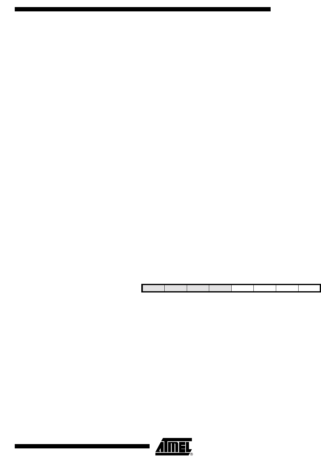
Bit 76543210
SRE SRW10 SE SM1 ISC11 ISC10 ISC01 ISC00 MCUCR
Read/Write R/W R/W R/W R/W R/W R/W R/W R/W
Initial Value00000000