
User guide


Table Of Contents
- Features
- Pin Configurations
- Overview
- AVR CPU Core
- AVR ATmega162 Memories
- System Clock and Clock Options
- Power Management and Sleep Modes
- System Control and Reset
- Interrupts
- I/O-Ports
- Introduction
- Ports as General Digital I/O
- Alternate Port Functions
- Register Description for I/O-Ports
- Port A Data Register – PORTA
- Port A Data Direction Register – DDRA
- Port A Input Pins Address – PINA
- Port B Data Register – PORTB
- Port B Data Direction Register – DDRB
- Port B Input Pins Address – PINB
- Port C Data Register – PORTC
- Port C Data Direction Register – DDRC
- Port C Input Pins Address – PINC
- Port D Data Register – PORTD
- Port D Data Direction Register – DDRD
- Port D Input Pins Address – PIND
- Port E Data Register – PORTE
- Port E Data Direction Register – DDRE
- Port E Input Pins Address – PINE
- External Interrupts
- 8-bit Timer/Counter0 with PWM
- Timer/Counter0, Timer/Counter1, and Timer/Counter3 Prescalers
- 16-bit Timer/Counter (Timer/Counter1 and Timer/Counter3)
- Restriction in ATmega161 Compatibility Mode
- Overview
- Accessing 16-bit Registers
- Timer/Counter Clock Sources
- Counter Unit
- Input Capture Unit
- Output Compare Units
- Compare Match Output Unit
- Modes of Operation
- Timer/Counter Timing Diagrams
- 16-bit Timer/Counter Register Description
- Timer/Counter1 Control Register A – TCCR1A
- Timer/Counter3 Control Register A – TCCR3A
- Timer/Counter1 Control Register B – TCCR1B
- Timer/Counter3 Control Register B – TCCR3B
- Timer/Counter1 – TCNT1H and TCNT1L
- Timer/Counter3 – TCNT3H and TCNT3L
- Output Compare Register 1 A – OCR1AH and OCR1AL
- Output Compare Register 1 B – OCR1BH and OCR1BL
- Output Compare Register 3 A – OCR3AH and OCR3AL
- Output Compare Register 3 B – OCR3BH and OCR3BL
- Input Capture Register 1 – ICR1H and ICR1L
- Input Capture Register 3 – ICR3H and ICR3L
- Timer/Counter Interrupt Mask Register – TIMSK(1)
- Extended Timer/Counter Interrupt Mask Register – ETIMSK(1)
- Timer/Counter Interrupt Flag Register – TIFR(1)
- Extended Timer/Counter Interrupt Flag Register – ETIFR(1)
- 8-bit Timer/Counter2 with PWM and Asynchronous operation
- Serial Peripheral Interface – SPI
- USART
- Analog Comparator
- JTAG Interface and On-chip Debug System
- IEEE 1149.1 (JTAG) Boundary-scan
- Boot Loader Support – Read-While-Write Self-programming
- Features
- Application and Boot Loader Flash Sections
- Read-While-Write and No Read-While-Write Flash Sections
- Boot Loader Lock Bits
- Entering the Boot Loader Program
- Addressing the Flash During Self- programming
- Self-programming the Flash
- Performing Page Erase by SPM
- Filling the Temporary Buffer (Page Loading)
- Performing a Page Write
- Using the SPM Interrupt
- Consideration while Updating BLS
- Prevent Reading the RWW Section During Self- programming
- Setting the Boot Loader Lock Bits by SPM
- EEPROM Write Prevents Writing to SPMCR
- Reading the Fuse and Lock Bits from Software
- Preventing Flash Corruption
- Programming Time for Flash When Using SPM
- Simple Assembly Code Example for a Boot Loader
- ATmega162 Boot Loader Parameters
- Memory Programming
- Program And Data Memory Lock Bits
- Fuse Bits
- Signature Bytes
- Calibration Byte
- Parallel Programming Parameters, Pin Mapping, and Commands
- Parallel Programming
- Enter Programming Mode
- Considerations for Efficient Programming
- Chip Erase
- Programming the Flash
- Programming the EEPROM
- Reading the Flash
- Reading the EEPROM
- Programming the Fuse Low Bits
- Programming the Fuse High Bits
- Programming the Extended Fuse Bits
- Programming the Lock Bits
- Reading the Fuse and Lock Bits
- Reading the Signature Bytes
- Reading the Calibration Byte
- Parallel Programming Characteristics
- Serial Downloading
- SPI Serial Programming Pin Mapping
- Programming via the JTAG Interface
- Programming Specific JTAG Instructions
- AVR_RESET (0xC)
- PROG_ENABLE (0x4)
- PROG_COMMANDS (0x5)
- PROG_PAGELOAD (0x6)
- PROG_PAGEREAD (0x7)
- Data Registers
- Reset Register
- Programming Enable Register
- Programming Command Register
- Virtual Flash Page Load Register
- Virtual Flash Page Read Register
- Programming Algorithm
- Entering Programming Mode
- Leaving Programming Mode
- Performing Chip Erase
- Programming the Flash
- Reading the Flash
- Programming the EEPROM
- Reading the EEPROM
- Programming the Fuses
- Programming the Lock Bits
- Reading the Fuses and Lock Bits
- Reading the Signature Bytes
- Reading the Calibration Byte
- Electrical Characteristics
- ATmega162 Typical Characteristics
- Active Supply Current
- Idle Supply Current
- Power-down Supply Current
- Power-save Supply Current
- Standby Supply Current
- Pin Pull-up
- Pin Driver Strength
- Pin Thresholds and Hysteresis
- BOD Thresholds and Analog Comparator Offset
- Internal Oscillator Speed
- Current Consumption of Peripheral Units
- Current Consumption in Reset and Reset Pulsewidth
- Register Summary
- Instruction Set Summary
- Ordering Information
- Packaging Information
- Erratas
- Datasheet Change Log for ATmega162
- Table of Contents
56
ATmega162/V
2513E–AVR–09/03
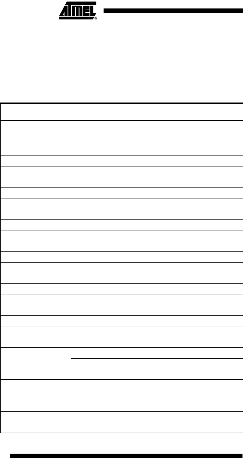
Interrupts This section describes the specifics of the interrupt handling as performed in
ATmega162. For a general explanation of the AVR interrupt handling, refer to “Reset
and Interrupt Handling” on page 12. Table 24 shows the interrupt table when the com-
patibility fuse (M161C) is unprogrammed, while Table 25 shows the interrupt table when
M161C Fuse is programmed. All assembly code examples in this sections are using the
interrupt table when the M161C Fuse is unprogrammed.
Interrupt Vectors in
ATmega162
Table 24. Reset and Interrupt Vectors if M161C is unprogrammed
Vector No.
Program
Address
(2)
Source Interrupt Definition
10x000
(1)
RESET External Pin, Power-on Reset, Brown-out
Reset, Watchdog Reset, and JTAG AVR
Reset
2 0x002 INT0 External Interrupt Request 0
3 0x004 INT1 External Interrupt Request 1
4 0x006 INT2 External Interrupt Request 2
5 0x008 PCINT0 Pin Change Interrupt Request 0
6 0x00A PCINT1 Pin Change Interrupt Request 1
7 0x00C TIMER3 CAPT Timer/Counter3 Capture Event
8 0x00E TIMER3 COMPA Timer/Counter3 Compare Match A
9 0x010 TIMER3 COMPB Timer/Counter3 Compare Match B
10 0x012 TIMER3 OVF Timer/Counter3 Overflow
11 0x014 TIMER2 COMP Timer/Counter2 Compare Match
12 0x016 TIMER2 OVF Timer/Counter2 Overflow
13 0x018 TIMER1 CAPT Timer/Counter1 Capture Event
14 0x01A TIMER1 COMPA Timer/Counter1 Compare Match A
15 0x01C TIMER1 COMPB Timer/Counter1 Compare Match B
16 0x01E TIMER1 OVF Timer/Counter1 Overflow
17 0x020 TIMER0 COMP Timer/Counter0 Compare Match
18 0x022 TIMER0 OVF Timer/Counter0 Overflow
19 0x024 SPI, STC Serial Transfer Complete
20 0x026 USART0, RXC USART0, Rx Complete
21 0x028 USART1, RXC USART1, Rx Complete
22 0x02A USART0, UDRE USART0 Data Register Empty
23 0x02C USART1, UDRE USART1 Data Register Empty
24 0x02E USART0, TXC USART0, Tx Complete
25 0x030 USART1, TXC USART1, Tx Complete
26 0x032 EE_RDY EEPROM Ready
27 0x034 ANA_COMP Analog Comparator
28 0x036 SPM_RDY Store Program Memory Ready