
User guide


Table Of Contents
- Features
- Pin Configurations
- Overview
- AVR CPU Core
- AVR ATmega162 Memories
- System Clock and Clock Options
- Power Management and Sleep Modes
- System Control and Reset
- Interrupts
- I/O-Ports
- Introduction
- Ports as General Digital I/O
- Alternate Port Functions
- Register Description for I/O-Ports
- Port A Data Register – PORTA
- Port A Data Direction Register – DDRA
- Port A Input Pins Address – PINA
- Port B Data Register – PORTB
- Port B Data Direction Register – DDRB
- Port B Input Pins Address – PINB
- Port C Data Register – PORTC
- Port C Data Direction Register – DDRC
- Port C Input Pins Address – PINC
- Port D Data Register – PORTD
- Port D Data Direction Register – DDRD
- Port D Input Pins Address – PIND
- Port E Data Register – PORTE
- Port E Data Direction Register – DDRE
- Port E Input Pins Address – PINE
- External Interrupts
- 8-bit Timer/Counter0 with PWM
- Timer/Counter0, Timer/Counter1, and Timer/Counter3 Prescalers
- 16-bit Timer/Counter (Timer/Counter1 and Timer/Counter3)
- Restriction in ATmega161 Compatibility Mode
- Overview
- Accessing 16-bit Registers
- Timer/Counter Clock Sources
- Counter Unit
- Input Capture Unit
- Output Compare Units
- Compare Match Output Unit
- Modes of Operation
- Timer/Counter Timing Diagrams
- 16-bit Timer/Counter Register Description
- Timer/Counter1 Control Register A – TCCR1A
- Timer/Counter3 Control Register A – TCCR3A
- Timer/Counter1 Control Register B – TCCR1B
- Timer/Counter3 Control Register B – TCCR3B
- Timer/Counter1 – TCNT1H and TCNT1L
- Timer/Counter3 – TCNT3H and TCNT3L
- Output Compare Register 1 A – OCR1AH and OCR1AL
- Output Compare Register 1 B – OCR1BH and OCR1BL
- Output Compare Register 3 A – OCR3AH and OCR3AL
- Output Compare Register 3 B – OCR3BH and OCR3BL
- Input Capture Register 1 – ICR1H and ICR1L
- Input Capture Register 3 – ICR3H and ICR3L
- Timer/Counter Interrupt Mask Register – TIMSK(1)
- Extended Timer/Counter Interrupt Mask Register – ETIMSK(1)
- Timer/Counter Interrupt Flag Register – TIFR(1)
- Extended Timer/Counter Interrupt Flag Register – ETIFR(1)
- 8-bit Timer/Counter2 with PWM and Asynchronous operation
- Serial Peripheral Interface – SPI
- USART
- Analog Comparator
- JTAG Interface and On-chip Debug System
- IEEE 1149.1 (JTAG) Boundary-scan
- Boot Loader Support – Read-While-Write Self-programming
- Features
- Application and Boot Loader Flash Sections
- Read-While-Write and No Read-While-Write Flash Sections
- Boot Loader Lock Bits
- Entering the Boot Loader Program
- Addressing the Flash During Self- programming
- Self-programming the Flash
- Performing Page Erase by SPM
- Filling the Temporary Buffer (Page Loading)
- Performing a Page Write
- Using the SPM Interrupt
- Consideration while Updating BLS
- Prevent Reading the RWW Section During Self- programming
- Setting the Boot Loader Lock Bits by SPM
- EEPROM Write Prevents Writing to SPMCR
- Reading the Fuse and Lock Bits from Software
- Preventing Flash Corruption
- Programming Time for Flash When Using SPM
- Simple Assembly Code Example for a Boot Loader
- ATmega162 Boot Loader Parameters
- Memory Programming
- Program And Data Memory Lock Bits
- Fuse Bits
- Signature Bytes
- Calibration Byte
- Parallel Programming Parameters, Pin Mapping, and Commands
- Parallel Programming
- Enter Programming Mode
- Considerations for Efficient Programming
- Chip Erase
- Programming the Flash
- Programming the EEPROM
- Reading the Flash
- Reading the EEPROM
- Programming the Fuse Low Bits
- Programming the Fuse High Bits
- Programming the Extended Fuse Bits
- Programming the Lock Bits
- Reading the Fuse and Lock Bits
- Reading the Signature Bytes
- Reading the Calibration Byte
- Parallel Programming Characteristics
- Serial Downloading
- SPI Serial Programming Pin Mapping
- Programming via the JTAG Interface
- Programming Specific JTAG Instructions
- AVR_RESET (0xC)
- PROG_ENABLE (0x4)
- PROG_COMMANDS (0x5)
- PROG_PAGELOAD (0x6)
- PROG_PAGEREAD (0x7)
- Data Registers
- Reset Register
- Programming Enable Register
- Programming Command Register
- Virtual Flash Page Load Register
- Virtual Flash Page Read Register
- Programming Algorithm
- Entering Programming Mode
- Leaving Programming Mode
- Performing Chip Erase
- Programming the Flash
- Reading the Flash
- Programming the EEPROM
- Reading the EEPROM
- Programming the Fuses
- Programming the Lock Bits
- Reading the Fuses and Lock Bits
- Reading the Signature Bytes
- Reading the Calibration Byte
- Electrical Characteristics
- ATmega162 Typical Characteristics
- Active Supply Current
- Idle Supply Current
- Power-down Supply Current
- Power-save Supply Current
- Standby Supply Current
- Pin Pull-up
- Pin Driver Strength
- Pin Thresholds and Hysteresis
- BOD Thresholds and Analog Comparator Offset
- Internal Oscillator Speed
- Current Consumption of Peripheral Units
- Current Consumption in Reset and Reset Pulsewidth
- Register Summary
- Instruction Set Summary
- Ordering Information
- Packaging Information
- Erratas
- Datasheet Change Log for ATmega162
- Table of Contents
205
ATmega162/V
2513E–AVR–09/03
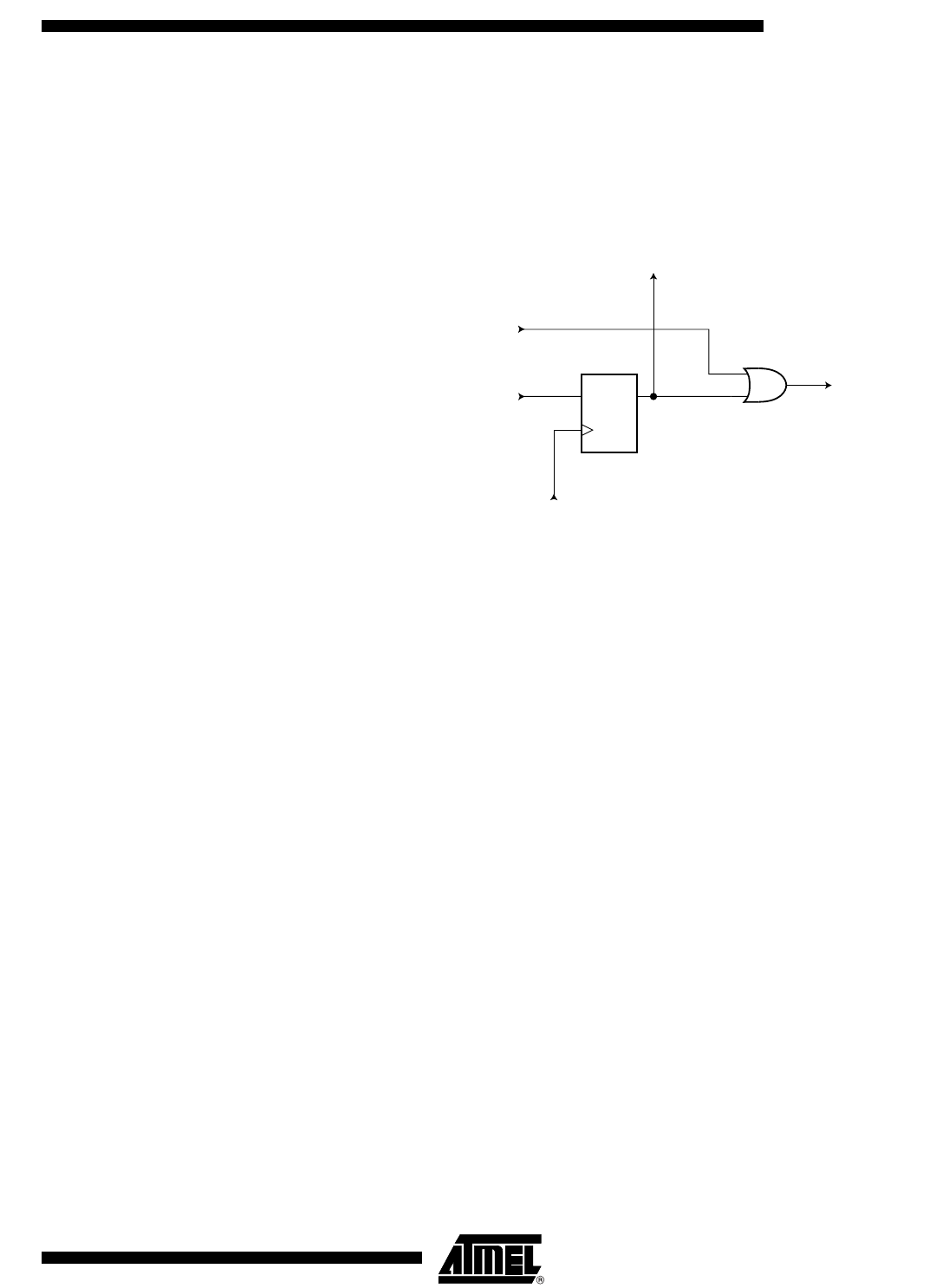
on the Fuse settings for the clock options, the part will remain reset for a Reset Time-out
Period (refer to “Clock Sources” on page 34) after releasing the Reset Register. The
output from this data register is not latched, so the reset will take place immediately, as
shown in Figure 86.
Figure 86. Reset Register
Boundary-scan Chain The Boundary-scan Chain has the capability of driving and observing the logic levels on
the digital I/O pins, as well as the boundary between digital and analog logic for analog
circuitry having Off-chip connections.
See “Boundary-scan Chain” on page 207 for a complete description.
Boundary-scan Specific
JTAG Instructions
The Instruction Register is 4-bit wide, supporting up to 16 instructions. Listed below are
the JTAG instructions useful for Boundary-scan operation. Note that the optional HIGHZ
instruction is not implemented, but all outputs with tri-state capability can be set in high-
impedant state by using the AVR_RESET instruction, since the initial state for all port
pins is tri-state.
As a definition in this datasheet, the LSB is shifted in and out first for all Shift Registers.
The OPCODE for each instruction is shown behind the instruction name in hex format.
The text describes which Data Register is selected as path between TDI and TDO for
each instruction.
EXTEST; 0x0 Mandatory JTAG instruction for selecting the Boundary-scan Chain as Data Register for
testing circuitry external to the AVR package. For port-pins, Pull-up Disable, Output
Control, Output Data, and Input Data are all accessible in the scan chain. For analog cir-
cuits having Off-chip connections, the interface between the analog and the digital logic
is in the scan chain. The contents of the latched outputs of the Boundary-scan chain is
driven out as soon as the JTAG IR-Register is loaded with the EXTEST instruction.
The active states are:
• Capture-DR: Data on the external pins are sampled into the Boundary-scan Chain.
• Shift-DR: The Internal Scan Chain is shifted by the TCK input.
• Update-DR: Data from the scan chain is applied to output pins.
DQ
From
TDI
ClockDR · AVR_RESET
To
TDO
From Other Internal and
External Reset Sources
Internal Reset