
User guide


Table Of Contents
- Features
- Pin Configurations
- Overview
- AVR CPU Core
- AVR ATmega162 Memories
- System Clock and Clock Options
- Power Management and Sleep Modes
- System Control and Reset
- Interrupts
- I/O-Ports
- Introduction
- Ports as General Digital I/O
- Alternate Port Functions
- Register Description for I/O-Ports
- Port A Data Register – PORTA
- Port A Data Direction Register – DDRA
- Port A Input Pins Address – PINA
- Port B Data Register – PORTB
- Port B Data Direction Register – DDRB
- Port B Input Pins Address – PINB
- Port C Data Register – PORTC
- Port C Data Direction Register – DDRC
- Port C Input Pins Address – PINC
- Port D Data Register – PORTD
- Port D Data Direction Register – DDRD
- Port D Input Pins Address – PIND
- Port E Data Register – PORTE
- Port E Data Direction Register – DDRE
- Port E Input Pins Address – PINE
- External Interrupts
- 8-bit Timer/Counter0 with PWM
- Timer/Counter0, Timer/Counter1, and Timer/Counter3 Prescalers
- 16-bit Timer/Counter (Timer/Counter1 and Timer/Counter3)
- Restriction in ATmega161 Compatibility Mode
- Overview
- Accessing 16-bit Registers
- Timer/Counter Clock Sources
- Counter Unit
- Input Capture Unit
- Output Compare Units
- Compare Match Output Unit
- Modes of Operation
- Timer/Counter Timing Diagrams
- 16-bit Timer/Counter Register Description
- Timer/Counter1 Control Register A – TCCR1A
- Timer/Counter3 Control Register A – TCCR3A
- Timer/Counter1 Control Register B – TCCR1B
- Timer/Counter3 Control Register B – TCCR3B
- Timer/Counter1 – TCNT1H and TCNT1L
- Timer/Counter3 – TCNT3H and TCNT3L
- Output Compare Register 1 A – OCR1AH and OCR1AL
- Output Compare Register 1 B – OCR1BH and OCR1BL
- Output Compare Register 3 A – OCR3AH and OCR3AL
- Output Compare Register 3 B – OCR3BH and OCR3BL
- Input Capture Register 1 – ICR1H and ICR1L
- Input Capture Register 3 – ICR3H and ICR3L
- Timer/Counter Interrupt Mask Register – TIMSK(1)
- Extended Timer/Counter Interrupt Mask Register – ETIMSK(1)
- Timer/Counter Interrupt Flag Register – TIFR(1)
- Extended Timer/Counter Interrupt Flag Register – ETIFR(1)
- 8-bit Timer/Counter2 with PWM and Asynchronous operation
- Serial Peripheral Interface – SPI
- USART
- Analog Comparator
- JTAG Interface and On-chip Debug System
- IEEE 1149.1 (JTAG) Boundary-scan
- Boot Loader Support – Read-While-Write Self-programming
- Features
- Application and Boot Loader Flash Sections
- Read-While-Write and No Read-While-Write Flash Sections
- Boot Loader Lock Bits
- Entering the Boot Loader Program
- Addressing the Flash During Self- programming
- Self-programming the Flash
- Performing Page Erase by SPM
- Filling the Temporary Buffer (Page Loading)
- Performing a Page Write
- Using the SPM Interrupt
- Consideration while Updating BLS
- Prevent Reading the RWW Section During Self- programming
- Setting the Boot Loader Lock Bits by SPM
- EEPROM Write Prevents Writing to SPMCR
- Reading the Fuse and Lock Bits from Software
- Preventing Flash Corruption
- Programming Time for Flash When Using SPM
- Simple Assembly Code Example for a Boot Loader
- ATmega162 Boot Loader Parameters
- Memory Programming
- Program And Data Memory Lock Bits
- Fuse Bits
- Signature Bytes
- Calibration Byte
- Parallel Programming Parameters, Pin Mapping, and Commands
- Parallel Programming
- Enter Programming Mode
- Considerations for Efficient Programming
- Chip Erase
- Programming the Flash
- Programming the EEPROM
- Reading the Flash
- Reading the EEPROM
- Programming the Fuse Low Bits
- Programming the Fuse High Bits
- Programming the Extended Fuse Bits
- Programming the Lock Bits
- Reading the Fuse and Lock Bits
- Reading the Signature Bytes
- Reading the Calibration Byte
- Parallel Programming Characteristics
- Serial Downloading
- SPI Serial Programming Pin Mapping
- Programming via the JTAG Interface
- Programming Specific JTAG Instructions
- AVR_RESET (0xC)
- PROG_ENABLE (0x4)
- PROG_COMMANDS (0x5)
- PROG_PAGELOAD (0x6)
- PROG_PAGEREAD (0x7)
- Data Registers
- Reset Register
- Programming Enable Register
- Programming Command Register
- Virtual Flash Page Load Register
- Virtual Flash Page Read Register
- Programming Algorithm
- Entering Programming Mode
- Leaving Programming Mode
- Performing Chip Erase
- Programming the Flash
- Reading the Flash
- Programming the EEPROM
- Reading the EEPROM
- Programming the Fuses
- Programming the Lock Bits
- Reading the Fuses and Lock Bits
- Reading the Signature Bytes
- Reading the Calibration Byte
- Electrical Characteristics
- ATmega162 Typical Characteristics
- Active Supply Current
- Idle Supply Current
- Power-down Supply Current
- Power-save Supply Current
- Standby Supply Current
- Pin Pull-up
- Pin Driver Strength
- Pin Thresholds and Hysteresis
- BOD Thresholds and Analog Comparator Offset
- Internal Oscillator Speed
- Current Consumption of Peripheral Units
- Current Consumption in Reset and Reset Pulsewidth
- Register Summary
- Instruction Set Summary
- Ordering Information
- Packaging Information
- Erratas
- Datasheet Change Log for ATmega162
- Table of Contents
204
ATmega162/V
2513E–AVR–09/03
Data Registers The data registers relevant for Boundary-scan operations are:
• Bypass Register
• Device Identification Register
• Reset Register
• Boundary-scan Chain
Bypass Register The Bypass Register consists of a single Shift Register stage. When the Bypass Regis-
ter is selected as path between TDI and TDO, the register is reset to 0 when leaving the
Capture-DR controller state. The Bypass Register can be used to shorten the scan
chain on a system when the other devices are to be tested.
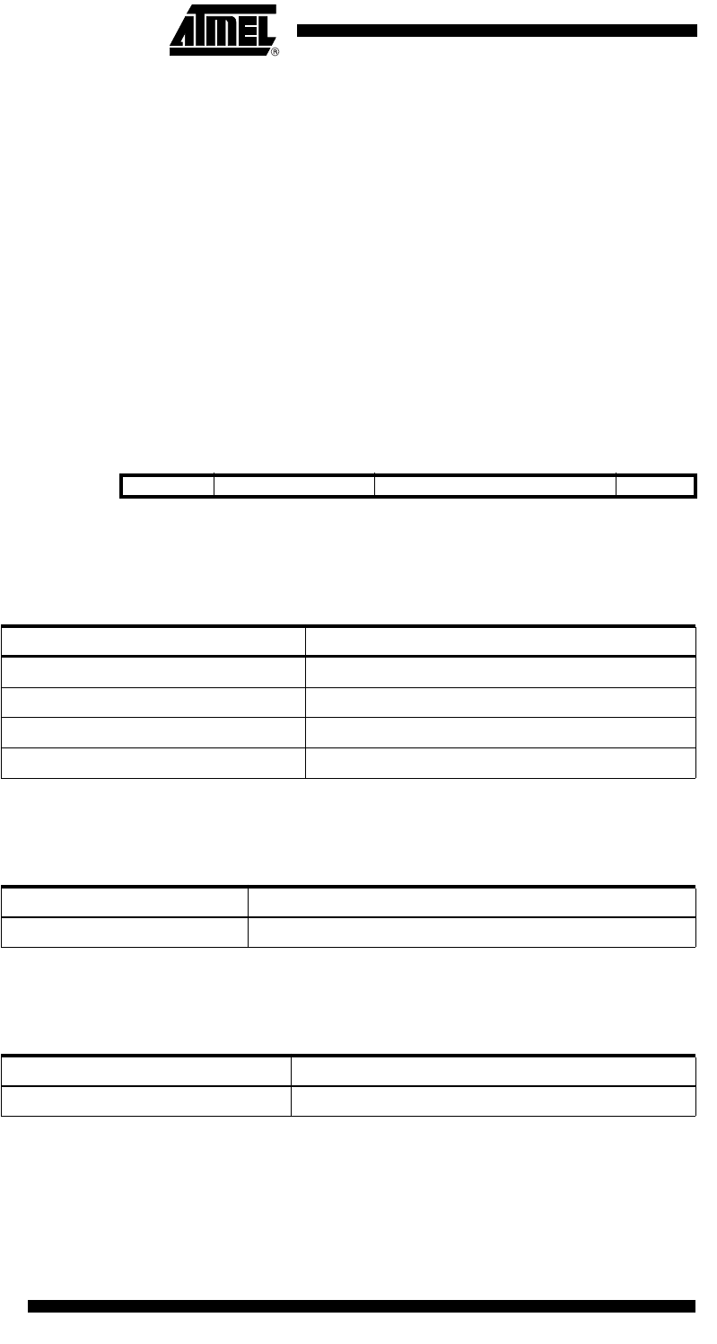
Device Identification Register Figure 85 shows the structure of the Device Identification Register.
Figure 85. The Format of the Device Identification Register
Version Version is a 4-bit number identifying the revision of the component. The relevant version
number is shown in Table 83.
Part Number The part number is a 16-bit code identifying the component. The JTAG Part Number for
ATmega162 is listed in Table 84.
Manufacturer ID The Manufacturer ID is a 11-bit code identifying the manufacturer. The JTAG manufac-
turer ID for ATMEL is listed in Table 85.
Reset Register The Reset Register is a test data register used to reset the part. Since the AVR tri-states
Port Pins when reset, the Reset Register can also replace the function of the unimple-
mented optional JTAG instruction HIGHZ.
A high value in the Reset Register corresponds to pulling the external Reset low. The
part is reset as long as there is a high value present in the Reset Register. Depending
MSB LSB
Bit 3128271211 1 0
Device ID Version Part Number Manufacturer ID 1
4 bits 16 bits 11 bits 1 bit
Table 83. JTAG Version Numbers
Version JTAG Version number (Hex)
ATmega162 revision A 0x0
ATmega162 revision B 0x1
ATmega162 revision C 0x2
ATmega162 revision D 0x3
Table 84. AVR JTAG Part Number
Part number JTAG Part Number (Hex)
ATmega162 0x9404
Table 85. Manufacturer ID
Manufacturer JTAG Man. ID (Hex)
ATMEL 0x01F