
User guide


Table Of Contents
- Features
- Pin Configurations
- Overview
- AVR CPU Core
- AVR ATmega162 Memories
- System Clock and Clock Options
- Power Management and Sleep Modes
- System Control and Reset
- Interrupts
- I/O-Ports
- Introduction
- Ports as General Digital I/O
- Alternate Port Functions
- Register Description for I/O-Ports
- Port A Data Register – PORTA
- Port A Data Direction Register – DDRA
- Port A Input Pins Address – PINA
- Port B Data Register – PORTB
- Port B Data Direction Register – DDRB
- Port B Input Pins Address – PINB
- Port C Data Register – PORTC
- Port C Data Direction Register – DDRC
- Port C Input Pins Address – PINC
- Port D Data Register – PORTD
- Port D Data Direction Register – DDRD
- Port D Input Pins Address – PIND
- Port E Data Register – PORTE
- Port E Data Direction Register – DDRE
- Port E Input Pins Address – PINE
- External Interrupts
- 8-bit Timer/Counter0 with PWM
- Timer/Counter0, Timer/Counter1, and Timer/Counter3 Prescalers
- 16-bit Timer/Counter (Timer/Counter1 and Timer/Counter3)
- Restriction in ATmega161 Compatibility Mode
- Overview
- Accessing 16-bit Registers
- Timer/Counter Clock Sources
- Counter Unit
- Input Capture Unit
- Output Compare Units
- Compare Match Output Unit
- Modes of Operation
- Timer/Counter Timing Diagrams
- 16-bit Timer/Counter Register Description
- Timer/Counter1 Control Register A – TCCR1A
- Timer/Counter3 Control Register A – TCCR3A
- Timer/Counter1 Control Register B – TCCR1B
- Timer/Counter3 Control Register B – TCCR3B
- Timer/Counter1 – TCNT1H and TCNT1L
- Timer/Counter3 – TCNT3H and TCNT3L
- Output Compare Register 1 A – OCR1AH and OCR1AL
- Output Compare Register 1 B – OCR1BH and OCR1BL
- Output Compare Register 3 A – OCR3AH and OCR3AL
- Output Compare Register 3 B – OCR3BH and OCR3BL
- Input Capture Register 1 – ICR1H and ICR1L
- Input Capture Register 3 – ICR3H and ICR3L
- Timer/Counter Interrupt Mask Register – TIMSK(1)
- Extended Timer/Counter Interrupt Mask Register – ETIMSK(1)
- Timer/Counter Interrupt Flag Register – TIFR(1)
- Extended Timer/Counter Interrupt Flag Register – ETIFR(1)
- 8-bit Timer/Counter2 with PWM and Asynchronous operation
- Serial Peripheral Interface – SPI
- USART
- Analog Comparator
- JTAG Interface and On-chip Debug System
- IEEE 1149.1 (JTAG) Boundary-scan
- Boot Loader Support – Read-While-Write Self-programming
- Features
- Application and Boot Loader Flash Sections
- Read-While-Write and No Read-While-Write Flash Sections
- Boot Loader Lock Bits
- Entering the Boot Loader Program
- Addressing the Flash During Self- programming
- Self-programming the Flash
- Performing Page Erase by SPM
- Filling the Temporary Buffer (Page Loading)
- Performing a Page Write
- Using the SPM Interrupt
- Consideration while Updating BLS
- Prevent Reading the RWW Section During Self- programming
- Setting the Boot Loader Lock Bits by SPM
- EEPROM Write Prevents Writing to SPMCR
- Reading the Fuse and Lock Bits from Software
- Preventing Flash Corruption
- Programming Time for Flash When Using SPM
- Simple Assembly Code Example for a Boot Loader
- ATmega162 Boot Loader Parameters
- Memory Programming
- Program And Data Memory Lock Bits
- Fuse Bits
- Signature Bytes
- Calibration Byte
- Parallel Programming Parameters, Pin Mapping, and Commands
- Parallel Programming
- Enter Programming Mode
- Considerations for Efficient Programming
- Chip Erase
- Programming the Flash
- Programming the EEPROM
- Reading the Flash
- Reading the EEPROM
- Programming the Fuse Low Bits
- Programming the Fuse High Bits
- Programming the Extended Fuse Bits
- Programming the Lock Bits
- Reading the Fuse and Lock Bits
- Reading the Signature Bytes
- Reading the Calibration Byte
- Parallel Programming Characteristics
- Serial Downloading
- SPI Serial Programming Pin Mapping
- Programming via the JTAG Interface
- Programming Specific JTAG Instructions
- AVR_RESET (0xC)
- PROG_ENABLE (0x4)
- PROG_COMMANDS (0x5)
- PROG_PAGELOAD (0x6)
- PROG_PAGEREAD (0x7)
- Data Registers
- Reset Register
- Programming Enable Register
- Programming Command Register
- Virtual Flash Page Load Register
- Virtual Flash Page Read Register
- Programming Algorithm
- Entering Programming Mode
- Leaving Programming Mode
- Performing Chip Erase
- Programming the Flash
- Reading the Flash
- Programming the EEPROM
- Reading the EEPROM
- Programming the Fuses
- Programming the Lock Bits
- Reading the Fuses and Lock Bits
- Reading the Signature Bytes
- Reading the Calibration Byte
- Electrical Characteristics
- ATmega162 Typical Characteristics
- Active Supply Current
- Idle Supply Current
- Power-down Supply Current
- Power-save Supply Current
- Standby Supply Current
- Pin Pull-up
- Pin Driver Strength
- Pin Thresholds and Hysteresis
- BOD Thresholds and Analog Comparator Offset
- Internal Oscillator Speed
- Current Consumption of Peripheral Units
- Current Consumption in Reset and Reset Pulsewidth
- Register Summary
- Instruction Set Summary
- Ordering Information
- Packaging Information
- Erratas
- Datasheet Change Log for ATmega162
- Table of Contents
201
ATmega162/V
2513E–AVR–09/03
On-chip debug specific
JTAG instructions
The On-chip debug support is considered being private JTAG instructions, and distrib-
uted within ATMEL and to selected 3rd party vendors only. Instruction opcodes are
listed for reference.
PRIVATE0; 0x8 Private JTAG instruction for accessing On-chip debug system.
PRIVATE1; 0x9 Private JTAG instruction for accessing On-chip debug system.
PRIVATE2; 0xA Private JTAG instruction for accessing On-chip debug system.
PRIVATE3; 0xB Private JTAG instruction for accessing On-chip debug system.
On-chip Debug Related
Register in I/O Memory
On-chip Debug Register –
OCDR
The OCDR Register provides a communication channel from the running program in the
microcontroller to the debugger. The CPU can transfer a byte to the debugger by writing
to this location. At the same time, an internal flag; I/O Debug Register Dirty – IDRD – is
set to indicate to the debugger that the register has been written. When the CPU reads
the OCDR Register the 7 LSB will be from the OCDR Register, while the MSB is the
IDRD bit. The debugger clears the IDRD bit when it has read the information.
In some AVR devices, this register is shared with a standard I/O location. In this case,
the OCDR Register can only be accessed if the OCDEN Fuse is programmed, and the
debugger enables access to the OCDR Register. In all other cases, the standard I/O
location is accessed.
Refer to the debugger documentation for further information on how to use this register.
Using the JTAG
Programming
Capabilities
Programming of AVR parts via JTAG is performed via the 4-pin JTAG port, TCK, TMS,
TDI and TDO. These are the only pins that need to be controlled/observed to perform
JTAG programming (in addition to power pins). It is not required to apply 12V externally.
The JTAGEN Fuse must be programmed and the JTD bit in the MCUSR Register must
be cleared to enable the JTAG Test Access Port.
The JTAG programming capability supports:
• Flash programming and verifying.
• EEPROM programming and verifying.
• Fuse programming and verifying.
• Lock bit programming and verifying.
The Lock bit security is exactly as in parallel programming mode. If the Lock bits LB1 or
LB2 are programmed, the OCDEN Fuse cannot be programmed unless first doing a
chip erase. This is a security feature that ensures no backdoor exists for reading out the
content of a secured device.
The details on programming through the JTAG interface and programming specific
JTAG instructions are given in the section “Programming via the JTAG Interface” on
page 249.
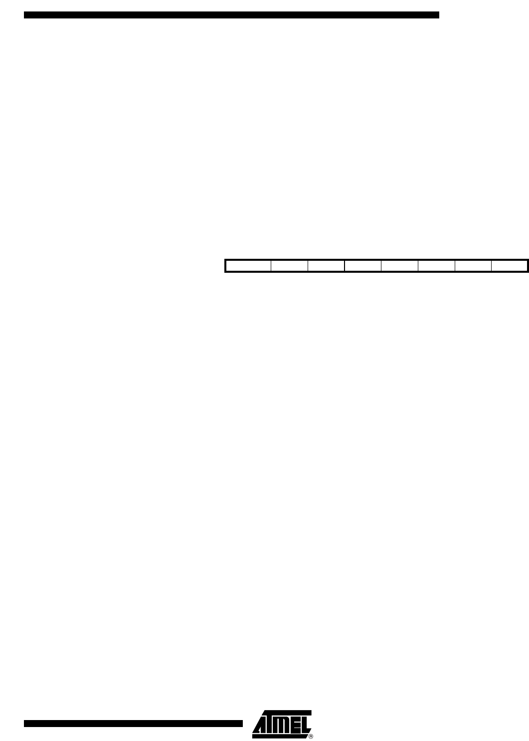
Bit 7 6543210
MSB/IDRD LSB OCDR
Read/Write R/W R/W R/W R/W R/W R/W R/W R/W
Initial Value0 0000000