
User guide


Table Of Contents
- Features
- Pin Configurations
- Overview
- AVR CPU Core
- AVR ATmega162 Memories
- System Clock and Clock Options
- Power Management and Sleep Modes
- System Control and Reset
- Interrupts
- I/O-Ports
- Introduction
- Ports as General Digital I/O
- Alternate Port Functions
- Register Description for I/O-Ports
- Port A Data Register – PORTA
- Port A Data Direction Register – DDRA
- Port A Input Pins Address – PINA
- Port B Data Register – PORTB
- Port B Data Direction Register – DDRB
- Port B Input Pins Address – PINB
- Port C Data Register – PORTC
- Port C Data Direction Register – DDRC
- Port C Input Pins Address – PINC
- Port D Data Register – PORTD
- Port D Data Direction Register – DDRD
- Port D Input Pins Address – PIND
- Port E Data Register – PORTE
- Port E Data Direction Register – DDRE
- Port E Input Pins Address – PINE
- External Interrupts
- 8-bit Timer/Counter0 with PWM
- Timer/Counter0, Timer/Counter1, and Timer/Counter3 Prescalers
- 16-bit Timer/Counter (Timer/Counter1 and Timer/Counter3)
- Restriction in ATmega161 Compatibility Mode
- Overview
- Accessing 16-bit Registers
- Timer/Counter Clock Sources
- Counter Unit
- Input Capture Unit
- Output Compare Units
- Compare Match Output Unit
- Modes of Operation
- Timer/Counter Timing Diagrams
- 16-bit Timer/Counter Register Description
- Timer/Counter1 Control Register A – TCCR1A
- Timer/Counter3 Control Register A – TCCR3A
- Timer/Counter1 Control Register B – TCCR1B
- Timer/Counter3 Control Register B – TCCR3B
- Timer/Counter1 – TCNT1H and TCNT1L
- Timer/Counter3 – TCNT3H and TCNT3L
- Output Compare Register 1 A – OCR1AH and OCR1AL
- Output Compare Register 1 B – OCR1BH and OCR1BL
- Output Compare Register 3 A – OCR3AH and OCR3AL
- Output Compare Register 3 B – OCR3BH and OCR3BL
- Input Capture Register 1 – ICR1H and ICR1L
- Input Capture Register 3 – ICR3H and ICR3L
- Timer/Counter Interrupt Mask Register – TIMSK(1)
- Extended Timer/Counter Interrupt Mask Register – ETIMSK(1)
- Timer/Counter Interrupt Flag Register – TIFR(1)
- Extended Timer/Counter Interrupt Flag Register – ETIFR(1)
- 8-bit Timer/Counter2 with PWM and Asynchronous operation
- Serial Peripheral Interface – SPI
- USART
- Analog Comparator
- JTAG Interface and On-chip Debug System
- IEEE 1149.1 (JTAG) Boundary-scan
- Boot Loader Support – Read-While-Write Self-programming
- Features
- Application and Boot Loader Flash Sections
- Read-While-Write and No Read-While-Write Flash Sections
- Boot Loader Lock Bits
- Entering the Boot Loader Program
- Addressing the Flash During Self- programming
- Self-programming the Flash
- Performing Page Erase by SPM
- Filling the Temporary Buffer (Page Loading)
- Performing a Page Write
- Using the SPM Interrupt
- Consideration while Updating BLS
- Prevent Reading the RWW Section During Self- programming
- Setting the Boot Loader Lock Bits by SPM
- EEPROM Write Prevents Writing to SPMCR
- Reading the Fuse and Lock Bits from Software
- Preventing Flash Corruption
- Programming Time for Flash When Using SPM
- Simple Assembly Code Example for a Boot Loader
- ATmega162 Boot Loader Parameters
- Memory Programming
- Program And Data Memory Lock Bits
- Fuse Bits
- Signature Bytes
- Calibration Byte
- Parallel Programming Parameters, Pin Mapping, and Commands
- Parallel Programming
- Enter Programming Mode
- Considerations for Efficient Programming
- Chip Erase
- Programming the Flash
- Programming the EEPROM
- Reading the Flash
- Reading the EEPROM
- Programming the Fuse Low Bits
- Programming the Fuse High Bits
- Programming the Extended Fuse Bits
- Programming the Lock Bits
- Reading the Fuse and Lock Bits
- Reading the Signature Bytes
- Reading the Calibration Byte
- Parallel Programming Characteristics
- Serial Downloading
- SPI Serial Programming Pin Mapping
- Programming via the JTAG Interface
- Programming Specific JTAG Instructions
- AVR_RESET (0xC)
- PROG_ENABLE (0x4)
- PROG_COMMANDS (0x5)
- PROG_PAGELOAD (0x6)
- PROG_PAGEREAD (0x7)
- Data Registers
- Reset Register
- Programming Enable Register
- Programming Command Register
- Virtual Flash Page Load Register
- Virtual Flash Page Read Register
- Programming Algorithm
- Entering Programming Mode
- Leaving Programming Mode
- Performing Chip Erase
- Programming the Flash
- Reading the Flash
- Programming the EEPROM
- Reading the EEPROM
- Programming the Fuses
- Programming the Lock Bits
- Reading the Fuses and Lock Bits
- Reading the Signature Bytes
- Reading the Calibration Byte
- Electrical Characteristics
- ATmega162 Typical Characteristics
- Active Supply Current
- Idle Supply Current
- Power-down Supply Current
- Power-save Supply Current
- Standby Supply Current
- Pin Pull-up
- Pin Driver Strength
- Pin Thresholds and Hysteresis
- BOD Thresholds and Analog Comparator Offset
- Internal Oscillator Speed
- Current Consumption of Peripheral Units
- Current Consumption in Reset and Reset Pulsewidth
- Register Summary
- Instruction Set Summary
- Ordering Information
- Packaging Information
- Erratas
- Datasheet Change Log for ATmega162
- Table of Contents
2
ATmega162/V
2513E–AVR–09/03
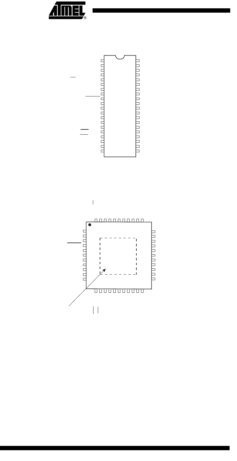
Pin Configurations Figure 1. Pinout ATmega162
Disclaimer Typical values contained in this datasheet are based on simulations and characteriza-
tion of other AVR microcontrollers manufactured on the same process technology. Min
and Max values will be available after the device is characterized.
(OC0/T0) PB0
(OC2/T1) PB1
(RXD1/AIN0) PB2
(TXD1/AIN1) PB3
(SS/OC3B) PB4
(MOSI) PB5
(MISO) PB6
(SCK) PB7
RESET
(RXD0) PD0
(TXD0) PD1
(INT0/XCK1) PD2
(INT1/ICP3) PD3
(TOSC1/XCK0/OC3A) PD4
(OC1A/TOSC2) PD5
(WR) PD6
(RD) PD7
XTAL2
XTAL1
GND
VCC
PA0 (AD0/PCINT0)
PA1 (AD1/PCINT1)
PA2 (AD2/PCINT2)
PA3 (AD3/PCINT3)
PA4 (AD4/PCINT4)
PA5 (AD5/PCINT5)
PA6 (AD6/PCINT6)
PA7 (AD7/PCINT7)
PE0 (ICP1/INT2)
PE1 (ALE)
PE2 (OC1B)
PC7 (A15/TDI/PCINT15)
PC6 (A14/TDO/PCINT14)
PC5 (A13/TMS/PCINT13)
PC4 (A12/TCK/PCINT12)
PC3 (A11/PCINT11)
PC2 (A10/PCINT10)
PC1 (A9/PCINT9)
PC0 (A8/PCINT8)
PA4 (AD4/PCINT4)
PA5 (AD5/PCINT5)
PA6 (AD6/PCINT6)
PA7 (AD7/PCINT7)
PE0 (ICP1/INT2)
GND
PE1 (ALE)
PE2 (OC1B)
PC7 (A15/TDI/PCINT15)
PC6 (A14/TDO/PCINT14)
PC5 (A13/TMS/PCINT13)
(MOSI) PB5
(MISO) PB6
(SCK) PB7
RESET
(RXD0) PD0
VCC
(TXD0) PD1
(INT0/XCK1) PD2
(INT1/ICP3) PD3
(TOSC1/XCK0/OC3A) PD4
(OC1A/TOSC2) PD5
(WR) PD6
(RD) PD7
XTAL2
XTAL1
GND
VCC
(A8/PCINT8) PC0
(A9/PCINT9) PC1
(A10/PCINT10) PC2
(A11/PCINT11) PC3
(TCK/A12/PCINT12) PC4
PB4 (SS/OC3B)
PB3 (TXD1/AIN1)
PB2 (RXD1/AIN0)
PB1 (OC2/T1)
PB0 (OC0/T0)
GND
VCC
PA0 (AD0/PCINT0)
PA1 (AD1/PCINT1)
PA2 (AD2/PCINT2)
PA3 (AD3/PCINT3)
40
39
38
37
36
35
34
33
32
31
30
29
28
27
26
25
24
23
22
21
1
2
3
4
5
6
7
8
9
10
11
12
13
14
15
16
17
18
19
20
PDIP
1
2
3
4
5
6
7
8
9
10
11
12 14 16 18 20 22
13 15 17 19 21
33
32
31
30
29
28
27
26
25
24
23
44 42 40 38 36 34
43 41 39 37 35
TQFP/MLF
NOTE:
MLF bottom pad should
be soldered to ground.