
User guide


Table Of Contents
- Features
- Pin Configurations
- Overview
- AVR CPU Core
- AVR ATmega162 Memories
- System Clock and Clock Options
- Power Management and Sleep Modes
- System Control and Reset
- Interrupts
- I/O-Ports
- Introduction
- Ports as General Digital I/O
- Alternate Port Functions
- Register Description for I/O-Ports
- Port A Data Register – PORTA
- Port A Data Direction Register – DDRA
- Port A Input Pins Address – PINA
- Port B Data Register – PORTB
- Port B Data Direction Register – DDRB
- Port B Input Pins Address – PINB
- Port C Data Register – PORTC
- Port C Data Direction Register – DDRC
- Port C Input Pins Address – PINC
- Port D Data Register – PORTD
- Port D Data Direction Register – DDRD
- Port D Input Pins Address – PIND
- Port E Data Register – PORTE
- Port E Data Direction Register – DDRE
- Port E Input Pins Address – PINE
- External Interrupts
- 8-bit Timer/Counter0 with PWM
- Timer/Counter0, Timer/Counter1, and Timer/Counter3 Prescalers
- 16-bit Timer/Counter (Timer/Counter1 and Timer/Counter3)
- Restriction in ATmega161 Compatibility Mode
- Overview
- Accessing 16-bit Registers
- Timer/Counter Clock Sources
- Counter Unit
- Input Capture Unit
- Output Compare Units
- Compare Match Output Unit
- Modes of Operation
- Timer/Counter Timing Diagrams
- 16-bit Timer/Counter Register Description
- Timer/Counter1 Control Register A – TCCR1A
- Timer/Counter3 Control Register A – TCCR3A
- Timer/Counter1 Control Register B – TCCR1B
- Timer/Counter3 Control Register B – TCCR3B
- Timer/Counter1 – TCNT1H and TCNT1L
- Timer/Counter3 – TCNT3H and TCNT3L
- Output Compare Register 1 A – OCR1AH and OCR1AL
- Output Compare Register 1 B – OCR1BH and OCR1BL
- Output Compare Register 3 A – OCR3AH and OCR3AL
- Output Compare Register 3 B – OCR3BH and OCR3BL
- Input Capture Register 1 – ICR1H and ICR1L
- Input Capture Register 3 – ICR3H and ICR3L
- Timer/Counter Interrupt Mask Register – TIMSK(1)
- Extended Timer/Counter Interrupt Mask Register – ETIMSK(1)
- Timer/Counter Interrupt Flag Register – TIFR(1)
- Extended Timer/Counter Interrupt Flag Register – ETIFR(1)
- 8-bit Timer/Counter2 with PWM and Asynchronous operation
- Serial Peripheral Interface – SPI
- USART
- Analog Comparator
- JTAG Interface and On-chip Debug System
- IEEE 1149.1 (JTAG) Boundary-scan
- Boot Loader Support – Read-While-Write Self-programming
- Features
- Application and Boot Loader Flash Sections
- Read-While-Write and No Read-While-Write Flash Sections
- Boot Loader Lock Bits
- Entering the Boot Loader Program
- Addressing the Flash During Self- programming
- Self-programming the Flash
- Performing Page Erase by SPM
- Filling the Temporary Buffer (Page Loading)
- Performing a Page Write
- Using the SPM Interrupt
- Consideration while Updating BLS
- Prevent Reading the RWW Section During Self- programming
- Setting the Boot Loader Lock Bits by SPM
- EEPROM Write Prevents Writing to SPMCR
- Reading the Fuse and Lock Bits from Software
- Preventing Flash Corruption
- Programming Time for Flash When Using SPM
- Simple Assembly Code Example for a Boot Loader
- ATmega162 Boot Loader Parameters
- Memory Programming
- Program And Data Memory Lock Bits
- Fuse Bits
- Signature Bytes
- Calibration Byte
- Parallel Programming Parameters, Pin Mapping, and Commands
- Parallel Programming
- Enter Programming Mode
- Considerations for Efficient Programming
- Chip Erase
- Programming the Flash
- Programming the EEPROM
- Reading the Flash
- Reading the EEPROM
- Programming the Fuse Low Bits
- Programming the Fuse High Bits
- Programming the Extended Fuse Bits
- Programming the Lock Bits
- Reading the Fuse and Lock Bits
- Reading the Signature Bytes
- Reading the Calibration Byte
- Parallel Programming Characteristics
- Serial Downloading
- SPI Serial Programming Pin Mapping
- Programming via the JTAG Interface
- Programming Specific JTAG Instructions
- AVR_RESET (0xC)
- PROG_ENABLE (0x4)
- PROG_COMMANDS (0x5)
- PROG_PAGELOAD (0x6)
- PROG_PAGEREAD (0x7)
- Data Registers
- Reset Register
- Programming Enable Register
- Programming Command Register
- Virtual Flash Page Load Register
- Virtual Flash Page Read Register
- Programming Algorithm
- Entering Programming Mode
- Leaving Programming Mode
- Performing Chip Erase
- Programming the Flash
- Reading the Flash
- Programming the EEPROM
- Reading the EEPROM
- Programming the Fuses
- Programming the Lock Bits
- Reading the Fuses and Lock Bits
- Reading the Signature Bytes
- Reading the Calibration Byte
- Electrical Characteristics
- ATmega162 Typical Characteristics
- Active Supply Current
- Idle Supply Current
- Power-down Supply Current
- Power-save Supply Current
- Standby Supply Current
- Pin Pull-up
- Pin Driver Strength
- Pin Thresholds and Hysteresis
- BOD Thresholds and Analog Comparator Offset
- Internal Oscillator Speed
- Current Consumption of Peripheral Units
- Current Consumption in Reset and Reset Pulsewidth
- Register Summary
- Instruction Set Summary
- Ordering Information
- Packaging Information
- Erratas
- Datasheet Change Log for ATmega162
- Table of Contents
141
ATmega162/V
2513E–AVR–09/03
resulting in incorrect Waveform Generation. Similarly, do not write the TCNT2 value
equal to BOTTOM when the counter is down-counting.
The Setup of the OC2 should be performed before setting the Data Direction Register
for the port pin to output. The easiest way of setting the OC2 value is to use the Force
Output Compare (FOC2) strobe bit in Normal mode. The OC2 Register keeps its value
even when changing between Waveform Generation modes.
Be aware that the COM21:0 bits are not double buffered together with the compare
value. Changing the COM21:0 bits will take effect immediately.
Compare Match Output
Unit
The Compare Output mode (COM21:0) bits have two functions. The waveform genera-
tor uses the COM21:0 bits for defining the Output Compare (OC2) state at the next
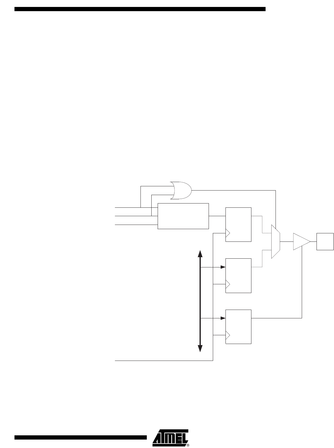
Compare Match. Also, the COM21:0 bits control the OC2 pin output source. Figure 62
shows a simplified schematic of the logic affected by the COM21:0 bit setting. The I/O
Registers, I/O bits, and I/O pins in the figure are shown in bold. Only the parts of the
general I/O Port Control Registers (DDR and PORT) that are affected by the COM21:0
bits are shown. When referring to the OC2 state, the reference is for the internal OC2
Register, not the OC2 pin.
Figure 62. Compare Match Output Unit, Schematic
The general I/O port function is overridden by the Output Compare (OC2) from the
waveform generator if either of the COM21:0 bits are set. However, the OC2 pin direc-
tion (input or output) is still controlled by the Data Direction Register (DDR) for the port
pin. The Data Direction Register bit for the OC2 pin (DDR_OC2) must be set as output
before the OC2 value is visible on the pin. The port override function is independent of
the Waveform Generation mode.
PORT
DDR
DQ
DQ
OCn
Pin
OCn
DQ
Waveform
Generator
COMn1
COMn0
0
1
DATA BUS
FOCn
clk
I/O